Laser Micromachining
Micron features. UV and IR.
355nm UV and 1064nm IR laser processing for micro-via drilling, precision cutting, dicing, and marking — built into the packaging flow, not bolted on after it.
/ 355nm UV / 1064nm IR / in-line with packaging / US-soil
What we do
Material removed where you want it. Nowhere else.
Two wavelengths cover the work: 355nm UV for tight, low-heat features in dielectrics and brittle materials; 1064nm IR for faster removal in metals and thicker stacks. We pick the source to the material and the feature, not the other way around.
- 01Micro-hole drilling — through-vias and blind vias, controlled depth and wall taper
- 02Precision cutting and structuring — profiles, slots, and edge features at micron scale
- 03Selective material removal and patterning — layer-specific ablation without disturbing what sits under it
- 04Dicing and singulation — clean kerf, low chipping, minimal heat-affected zone
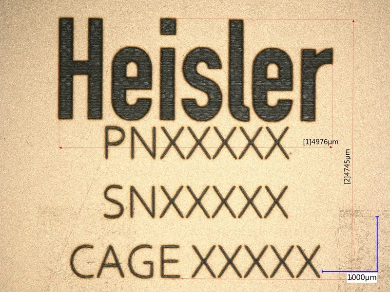
- 05Part marking and traceability — permanent, legible IDs on production parts
- 06Preform fabrication — shaped material blanks cut to spec for downstream assembly
Beam, pulse, and fluence parameters set per material and feature — process windows shared under NDA.
A non-contact tool means no fixturing damage.
Laser ablation puts no mechanical load on the part. There is no blade to chip a die edge, no drill to wander, no contact to crack a thin or brittle substrate.
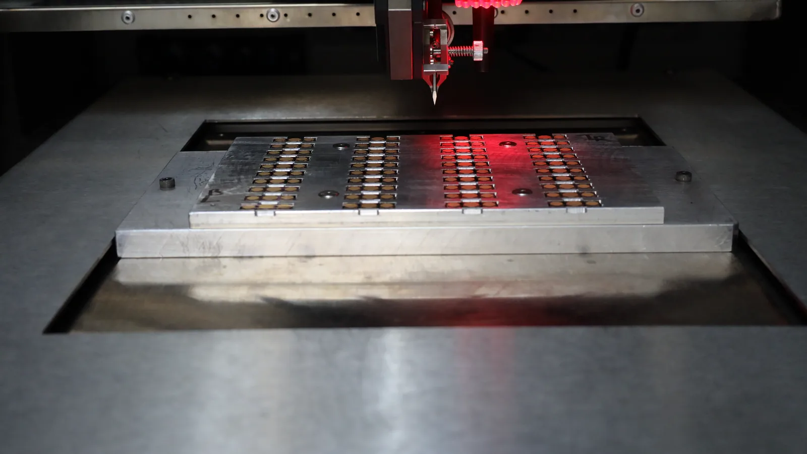
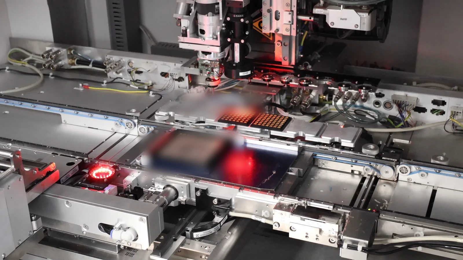
That matters most on the materials advanced packaging actually runs — thinned silicon, sapphire, ceramics. Tight pulse control keeps the heat-affected zone small, so vias and cuts stay dimensionally honest and adjacent layers stay intact. Because the laser cell lives in the same flow as die attach, wafer-level, and inspection, parts move between steps without an external hand-off and without leaving US soil.
Two sources, one cell
UV and IR · wavelength matched to material and feature
Full process detail, tolerances, and qualification data available under NDA.
Materials and applications
What it cuts. Where it goes.
Materials
- ·Silicon
- ·Sapphire
- ·Ceramics
- ·Metals and specialty alloys
- ·Polymers
Applications
- ·TSV and microvia in silicon
- ·Interposers
- ·Micro-fluidic features
- ·Part marking and traceability
Feature geometry, tolerances, and qualification data available under NDA.
How we engage
Send the feature. We size the process.
Give us the material, the geometry, and the tolerance you need to hold. We map it to a wavelength and a process window, prove it on representative material, and fold the laser step into the rest of your build — design review through volume, one engineering team.
Built into the rest of the flow.
Process More.
Bring us the feature that
won't drill cleanly.
UV and IR under one roof, in-line with packaging. Request a capability brief for process windows, tolerances, and qualification data under NDA.
/ US-soil / ITAR-aware / in-line with packaging