Advanced Packaging / US Die Bonding
US die bonding, placed to two
and a half microns.
Die attach and die bonding at ±2.5µm @3σ — epoxy, eutectic, sinter and fluxless, die-to-wafer through die-to-PCB, on US soil with placement data captured per unit.
/ ±2.5µm @3σ / Wafer 2″–12″ / US-soil
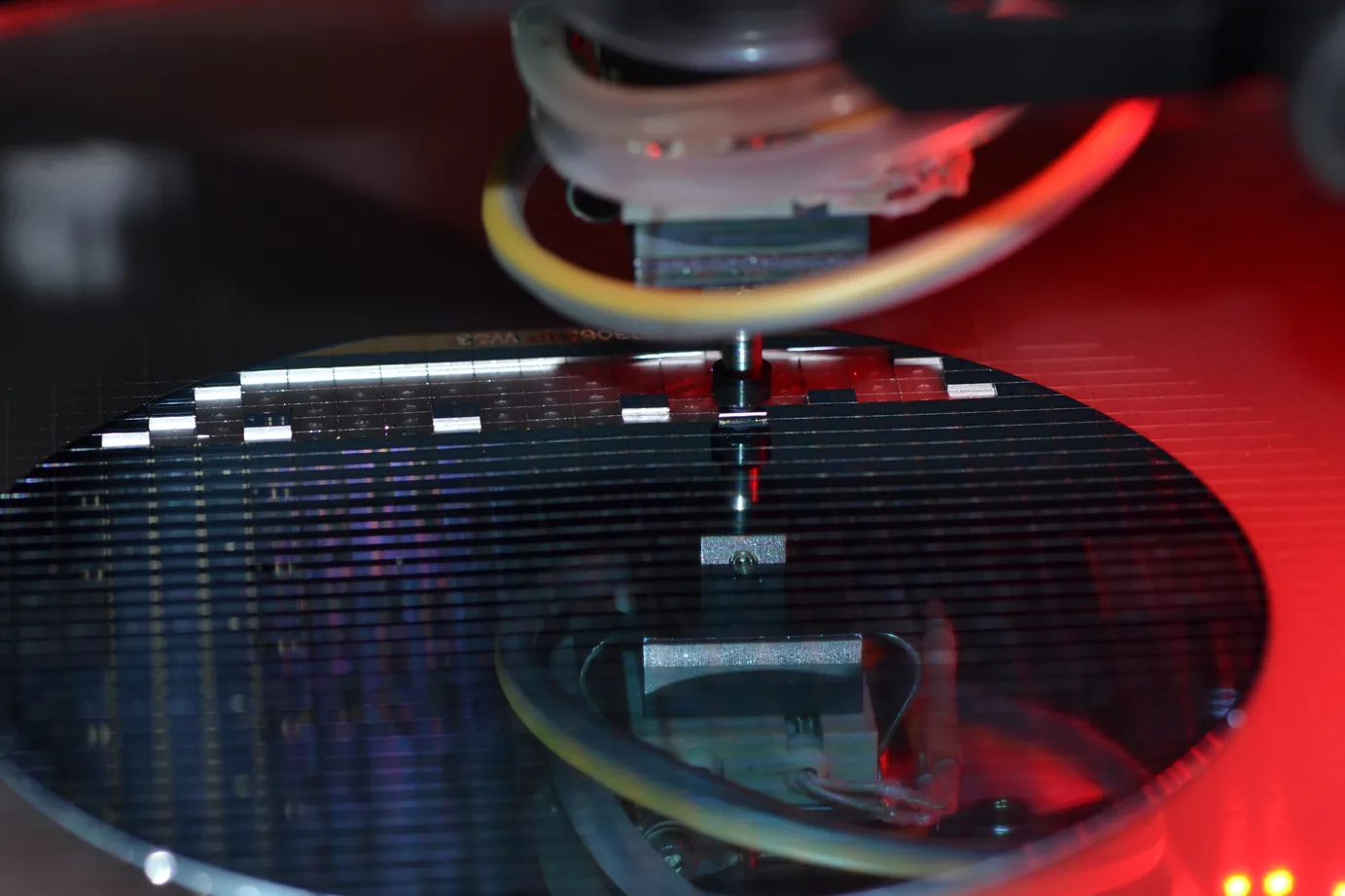
BESI Datacon & Tresky — per-build placement data
Panel-level die attach, no post-attach clean
Wafer sizes handled, including thin die
Attach methods · matched to your stack
Full process detail, design rules, and build data available under NDA.
What we do
The attach step, done four ways.
Die attach decides thermal path, electrical contact, and how the package survives reliability. We pick the method against your requirements — not a house default.
Epoxy
Conductive & non-conductive
Fast, forgiving die attach for general assembly, sensors, and prototypes — cured and characterized for void control.
Eutectic
Au-based, void-controlled
For high-thermal-path and hermetic builds where a metallurgical bond and low void fraction matter.
Sinter
Silver, high-temp
Pressure or pressureless silver sinter for power and high-temperature operation that outlasts solder.
Fluxless
Maskless, clean
No-clean attach for sensitive die and RF surfaces — proven fluxless, maskless on AlN at 100% yield.
Configurations
- 01Die-to-wafer — reconstituted and known-good-die builds
- 02Die-to-die — stacked and side-by-side
- 03Die-to-substrate — ceramic, AlN, organic interposer
- 04Die-to-PCB — chip-on-board into the final assembly
Die & substrate range
- 05Wafer 2″ through 12″, including thin and fragile die
- 06Si (CMOS-compatible), sapphire, AlN, ceramic carriers
- 07Small-pitch, multi-die, and mixed-die-size layouts
- 08Hermetic-ready and reliability-screened builds
Accuracy & tooling
Accuracy you can audit.
±2.5µm @3σ is a measured number, not a brochure claim. Every placement is captured, so the data backs the spec before your unit ships.
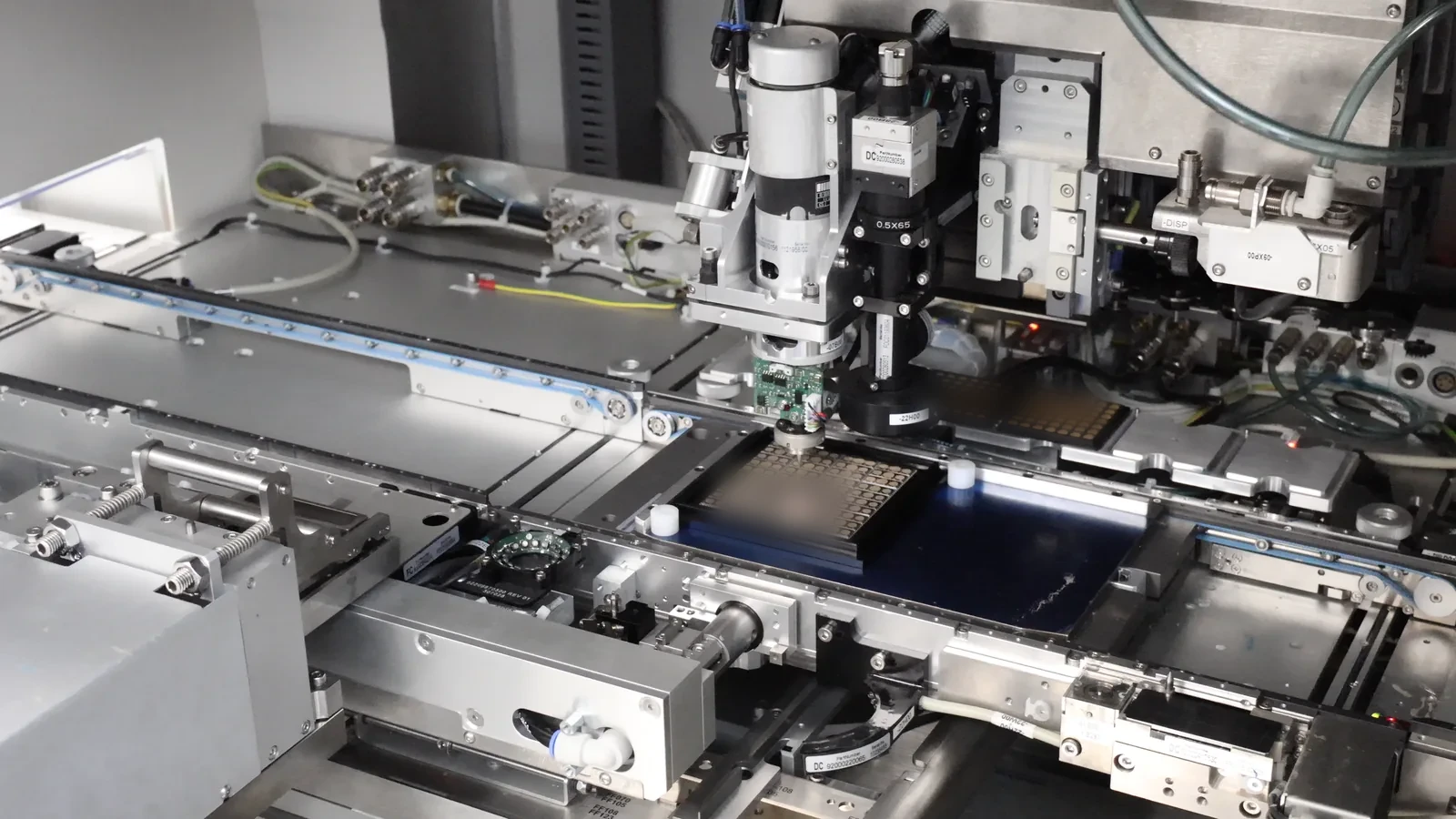
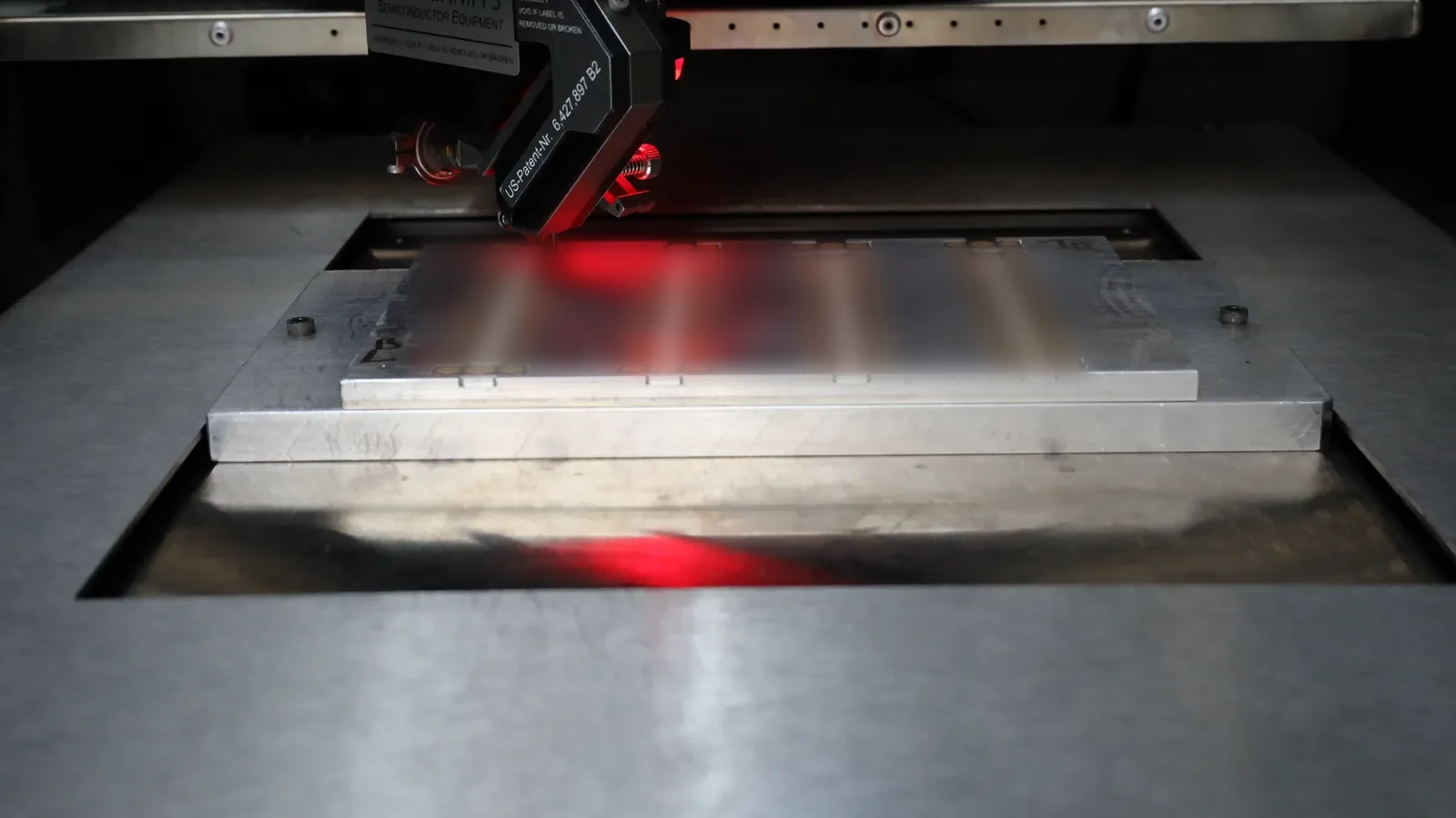
BESI Datacon — high-accuracy automated die bonding
Tresky — flexible manual / semi-auto attach & R&D
Placement-data capture — per-unit X/Y/θ logged for SPC
Vision-aligned placement with fiducial and edge referencing for tight, repeatable position.
Bond-line, force and temperature profiles tuned per attach method and die size.
Placement data captured per unit and fed straight into SPC and yield tracking.
Post-attach inspection — die-attach void content verified by X-ray when void measurement is required, plus AOI, metrology, and die-shear strength testing to MIL-STD-883 Method 2019 when required — closes the loop.
Anyone can place a die.
Developing the attach is the work.
A new die attach — new die, new substrate, new thermal budget — rarely works on the first recipe. We get it to a stable, documented process window before it costs you a build.
We run attach development as a DOE-driven, SPC-controlled engineering loop: define objectives, build a test vehicle, run the experiment, validate with real metrology, and document the window. See how we develop process with data and AI across every build.
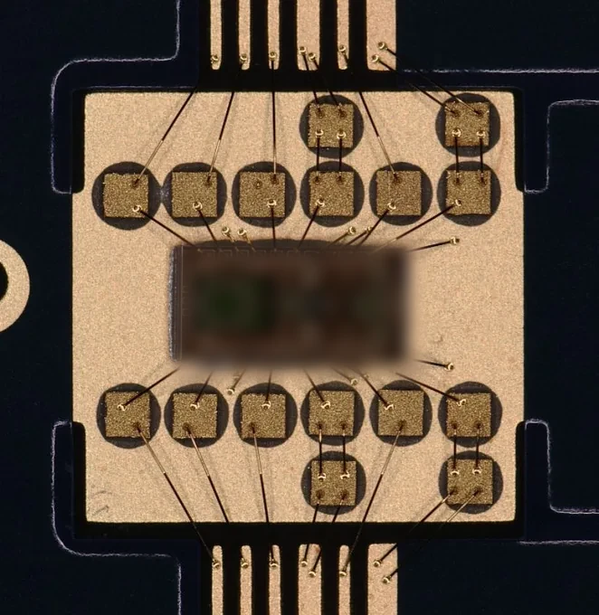
Stacked die & 3D
From one die to a stack.
Tight placement is what makes stacked-die and 3D builds manufacturable. Hold ±2.5µm at the attach step and the interconnect step above it has room to work.
Die attach is the foundation under multi-die modules, interposer stacks, and 3D heterogeneous integration. It pairs with wire bond, hermetic packaging, 3D heterogeneous integration and flip chip as part of one advanced packaging flow under a single engineering team.
Where it fits
Built for hard hardware.
Aerospace & Defense
MIL-STD qualification available, hermetic-ready, US-soil.
Medical & Bio
Small, reliable die attach for implantable-class and sensor builds.
RF & mmWave
Fluxless, low-parasitic attach on AlN and ceramic for RF surfaces.
Advanced Sensors
Thin, fragile, and MEMS die placed at panel scale, 100% yield.
Die attach, answered.
Where can I get die bonding services in the US?
Here. Heisler runs die bonding in-house near Baltimore, Maryland — every die is placed, attached, and inspected on US soil, with MIL-STD qualification available. No overseas hand-off in the middle of your build.
What die placement accuracy can you hold?
We place die to ±2.5µm @3σ on BESI Datacon and Tresky bonders, with placement data captured per unit so the accuracy is proven, not asserted.
Which die attach methods do you support?
Epoxy, eutectic, silver sinter, and fluxless. We select the method against your thermal, electrical, reliability and downstream-process requirements rather than defaulting to one recipe.
When should I choose eutectic versus epoxy die attach?
Epoxy attach cures at lower temperature and is fast and forgiving, a strong fit for general assembly, sensors, and prototypes, in conductive or non-conductive forms. Eutectic attach forms a metallurgical, void-controlled bond with the highest thermal and electrical path for high-power and hermetic builds, at a higher process temperature and bond-line stress. We select against your thermal budget, reliability target, and downstream steps rather than defaulting to one recipe.
How do you verify die-attach quality and voids?
Post-attach, we inspect the bond with AOI and metrology, and verify die-attach void content by X-ray inspection when void measurement is required — per your spec or customer requirement, plus die-shear strength testing to MIL-STD-883 Method 2019 for mechanical acceptance when required. Placement is captured per unit for SPC, so the attach is proven, not asserted.
What configurations and wafer sizes do you handle?
Die-to-wafer, die-to-die, die-to-substrate, and die-to-PCB. Wafer sizes from 2″ to 12″, including thin and fragile die and stacked-die builds for 3D heterogeneous integration.
Can you develop a new die attach process, not just run one?
Yes. We run attach development as a DOE-driven, SPC-controlled loop — objectives, test vehicle, experiment, metrology validation, documented window — before scale-up.
Is the work done in the United States?
Yes. All die attach is performed on US soil, with MIL-STD qualification available when the program requires it.
Process More.
Send us the die that
has to land right.
One engineering team, design review through volume. Request a capability brief for attach-method selection, design rules, and build data under NDA.
/ ±2.5µm @3σ / US-soil / traceable