ASIC Packaging & Test
Bare die to a characterized, US-made module.
You taped out. Now the die has to become a package, an assembly, and a tested module. We run everything downstream of bare silicon on US soil – die attach, wire bond, flip chip, wafer- and panel-level, hermetic seal, and characterization – at low minimums, with engineers on the program from test vehicle to volume.
/ MIL-STD-883 workmanship / ITAR-aware / US-soil
Proof / Wire-bond pull test
Bonds pulled to MIL-STD-883.
Engineers judge a packaging house on data, not adjectives. A representative batch of 44 wire bonds, destructively pull-tested to MIL-STD-883 Method 2011, held a mean of 3.9× the standard minimum – the weakest single bond still cleared it at 2.6×.
Bonds pull-tested
Mean vs. minimum
Weakest bond
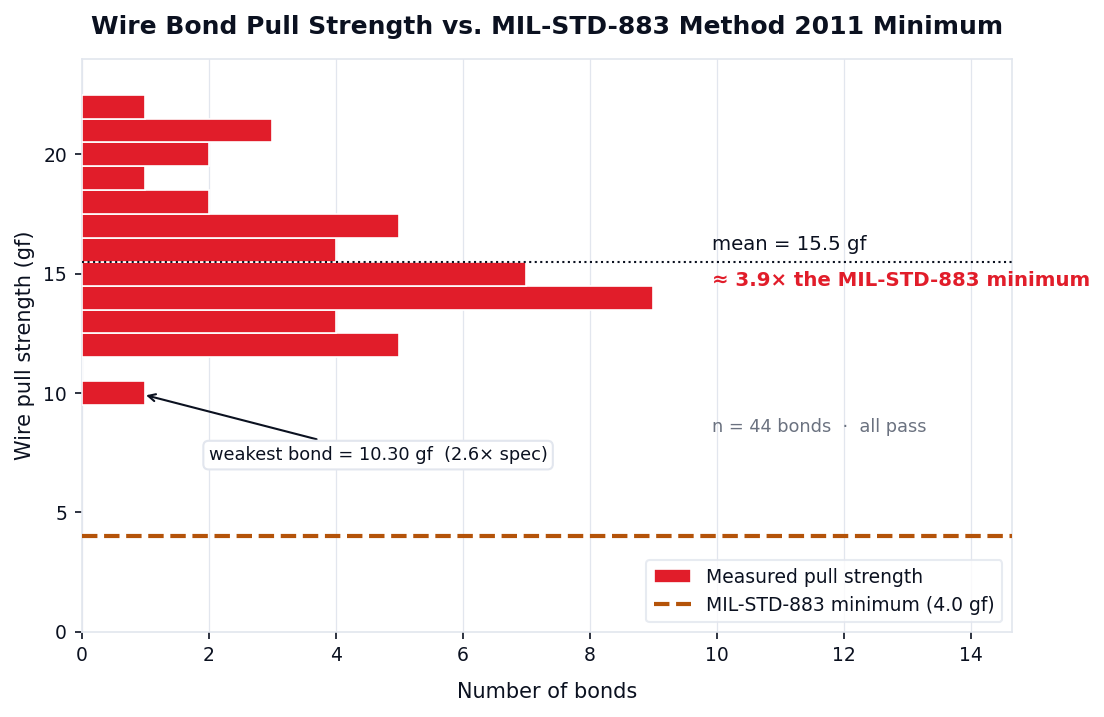
Representative pull-test batch (n=44) against the MIL-STD-883 Method 2011 minimum. De-identified; full pull and shear distributions available under NDA.
What we do / For a taped-out chip
Everything downstream of bare die.
Hand us wafers or singulated die. We take the process from there through a tested module, assembled through our advanced packaging line.
- 01Die attach – eutectic and epoxy; SiC, GaN, and AlN substrates
- 02Wire bond – gold ball and aluminum wedge, 15–50 µm, thermosonic and ultrasonic
- 03Flip chip – bumped-die attach, reflow, and underfill
- 04Wafer- and panel-level packaging
- 053D, chiplet and heterogeneous integration
- 06Hermetic sealing and leak test
- 07Characterization and inspection – SEM, X-ray, and AOI, engineer-reviewed
- 08Eval and demo board design and realization – the board your customers run the die on
Material systems, bond recipes, and step-level routing available under NDA.
Why it matters / For fabless teams
Skip the line you'd have to build yourself.
Standing up a packaging line burns time and capital you'd rather spend on the next design. Sending die offshore adds export risk and a queue you don't control. We are the third option.
- 01No packaging line to stand up – we are your downstream, capital-light
- 02US soil, ITAR-aware – defense-adjacent programs welcome
- 03Low minimums – first silicon and startup volumes, not MOQ walls
- 04Engineers on the program – from test-vehicle design through volume
Who it's for
Built for teams that ship silicon.
Fabless & ASIC
IC design houses and ASIC startups that have taped out and need the die packaged, assembled, and tested.
RF & mmWave
GaN and GaAs devices where die attach, bond, and thermal path decide the part's performance.
Advanced sensors
MEMS, imaging, and sensor die that need cavity packages, controlled seals, and careful handling.
Defense-adjacent
Programs that need a US-soil, ITAR-aware path with MIL-STD workmanship and traceability.
ASIC packaging and test, answered.
What does an ASIC packaging and test house do?
It takes a taped-out chip through everything downstream of the wafer: die attach, wire bond or flip chip, wafer- and panel-level packaging, 3D and chiplet integration, hermetic sealing, and the characterization and inspection that turn bare die into a tested module. We do that on US soil at low minimums.
Can you do chiplet or heterogeneous integration?
Yes. We build 3D, chiplet, and heterogeneous integration – multiple die and materials combined in one package – alongside wafer- and panel-level packaging and flip chip, so a multi-die module is assembled and tested by one engineering team.
Do you take low volumes or first silicon?
Yes. We work at startup and first-silicon volumes, not high MOQ walls. A fabless team can bring first die for a test vehicle and characterization, then scale the same flow toward volume with the same engineers.
Is the work done in the United States?
Yes. Assembly, packaging, and test are performed on US soil with an ITAR-aware process and MIL-STD-883 workmanship, so defense-adjacent programs can avoid offshore export risk.
Process More.
Send us your die. Get back a tested module.
Bare die to a characterized, US-made module – assembly, packaging, and test under one engineering team. Request a capability brief for material systems, bond and seal data, and the flow that fits your part, under NDA.
/ US-soil / ITAR-aware / MIL-STD-883