Industries / Advanced Sensors
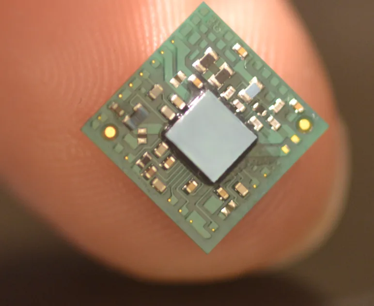
Advanced Sensor Packaging.
Not Just the Die.
Wafer- and panel-level packaging for MEMS, photonic and optical sensors, imaging arrays, IR and thermal detectors, and microfluidic bio sensors – developed, sealed, and inspected by one US engineering team.
/ wafer-level & panel-level / vacuum & cavity seal / sub-micron metrology / US-soil
A sensor lives or dies
at the package.
The transducer is only half the part. Whether a MEMS membrane, a photodiode array, or a microfluidic channel survives reflow, handling, and the field comes down to how it is sealed, stacked, and singulated.
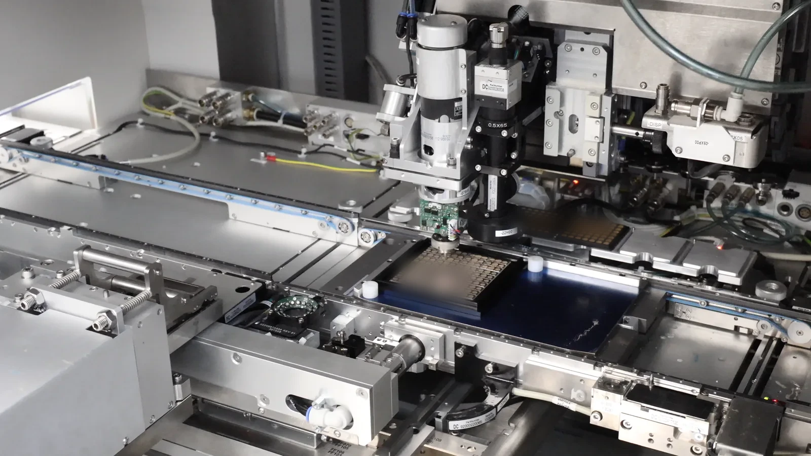
We treat sensor packaging as a process-development problem: define the objective, build a test vehicle, run the DOE, and validate against real metrology before the build scales. The result is a package that protects the sensing element, holds optical or fluidic alignment, and repeats across a panel – not a one-off that yields once.
Proof, from real sensor builds
Yield at panel scale isn’t a target. It’s the record.
MEMS assemblies · panel-level · 100% yield · no post-attach clean
MEMS, IMU, pressure, optical sensors assembled
Panel-level assembly, no post-attach clean
Full design rules, process detail, and build data available under NDA.
Capabilities mapped to the sensor
From transducer
to qualified part.
MEMS, photonics, imaging, IR, and bio sensors share one problem: the sensing element is fragile, alignment-critical, and unforgiving of contamination. The packaging methods below are built for exactly that.
Developed in-house, inspected in-house, and qualified to your requirement – one engineering team from first test vehicle through volume.
- 01Wafer-level packaging – WLP and fan-out on 2″–12″ wafers, RDL and interposers for compact sensor stacks. Wafer-level →
- 02MEMS panel-level assembly – high-volume die attach across a panel with ±2.5µm placement, no post-attach clean. Advanced packaging →
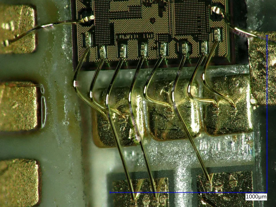
- 03Vacuum & controlled-atmosphere cavities – sealed cavities for MEMS, IR detectors, and resonators that must hold pressure or vacuum over life, sealed and leak-tested through our hermetic sensor packaging line.
- 04Laser micromachining – UV 355nm and IR 1064nm micro-vias, dicing, and singulation on Si, sapphire, ceramics, and polymers without stressing the sensing element. Laser micromachining →
- 05Optical & photonic packaging – fine-pitch die attach and flip chip that holds alignment for photodiode arrays, imaging sensors, and optical sources.
- 06Microfluidic & bio sensor assembly – channel and cap integration for lab-on-chip and bio-sensing devices. Medical & bio →
- 07Inspection & metrology – X-ray, 3D AOI, SEM, sub-micron metrology, and cross-section – the data behind every yield claim. Inspection & metrology →
Materials: Si (CMOS-compatible), sapphire, quartz, AlN, polyimide, thin-film metallization. Deeper design rules under NDA.
Why it matters
Yield, miniaturization,
and a part that survives.
- 01High-volume yield. Panel-level assembly turns a fragile sensor into a repeatable part – 4,000+ MEMS units at 100% yield is the kind of record a production program is built on.
- 02Miniaturization. Wafer-level packaging, RDL, and 3D stacking pack more sensing into less size, weight, and power – without giving up the seal.
- 03Harsh-environment reliability. Vacuum and controlled-atmosphere sealing plus thermal cycling and screening keep the sensing element working through temperature, vibration, and humidity.
- 04Traceable data. Process, inspection, metrology, and test captured per build – defensible when a customer or auditor asks how the part was qualified.
A sensor that yields in the lab and fails at panel scale isn’t a product.
We close that gap with process development and metrology, so the part that ships is the part you qualified – at the volume your roadmap needs.
How we engage
Scoped, under NDA,
engineer to engineer.
We talk to your engineers, not just procurement.
Tell us the sensor, the environment it has to survive, and the volume you need. We’ll tell you what’s feasible, where the risk is, and what it takes to retire it – before you commit the program. Want the data engine first? Start with inspection & metrology.
Process More.
Bring us the sensor
that has to ship at volume.
Wafer- and panel-level packaging, sealed and qualified on US soil. Request a capability brief for design rules, full process detail, and build data under NDA.
/ wafer-level / panel-level / US-soil