Advanced Packaging / Flip Chip
Flip chip, fully characterized.
C4 solder, C2 copper-pillar, Au-stud, and micro-bump interconnect — six attach families run in-house, with capillary, no-flow, or ACF underfill. Wafer-level and panel-level bumping on US soil, one engineering team from design-rule review through qualified volume.
/ ±2.5µm @3σ placement / SPC-controlled / MIL-STD when required
Proof, from real flip-chip builds
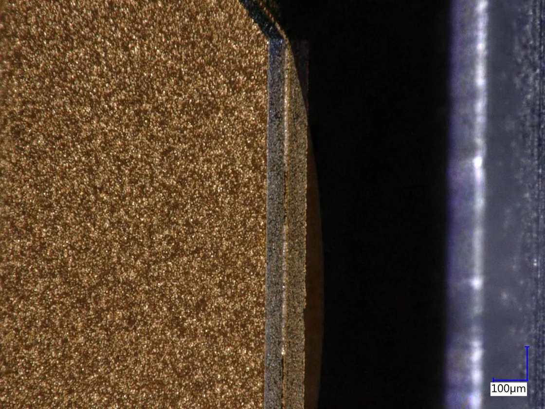
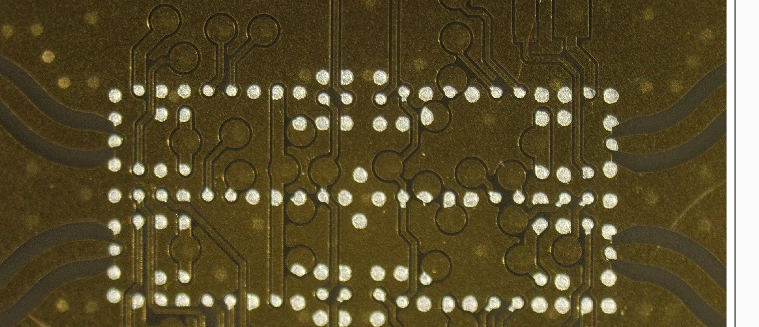
Bumps in a single C4 package · 60µm bump · 100µm pitch · SAC305 · 100% production yield
Interconnect / attach families run in-house — ACA, ICA, NCA, solder, TC, TS
MEMS assemblies, panel-level at 100% yield with no post-attach clean
Full process detail and design rules available under NDA.
Bump & interconnect
Pick by pitch. All in-house.
Four bump types, three underfill flows, and four die-attach targets — the full flip-chip menu runs under one roof, so the right interconnect gets chosen at design review, not forced by what a vendor can do.
Above ~100 I/O the question stops being interesting: flip chip is the path. Below it, we still flip-chip when parasitic inductance, thermal dissipation, or footprint drive the call.
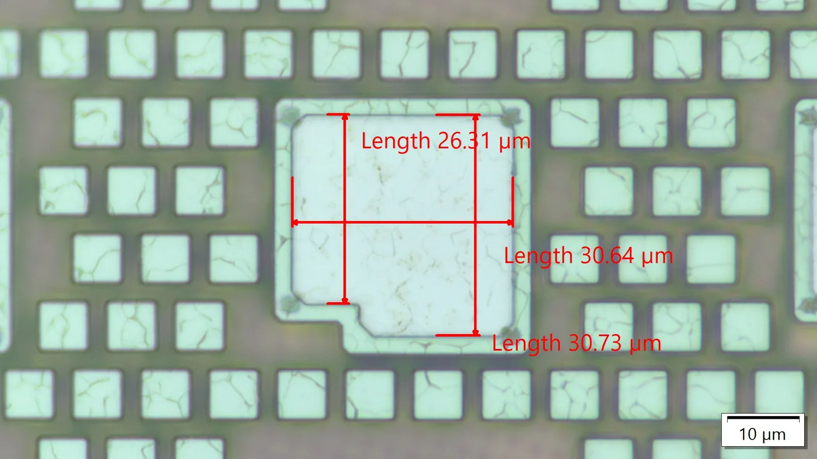
- 01C4 solder bump — SAC305 mass-reflow workhorse for >130µm pitch. Self-aligning under reflow; underfill on laminate.
- 02C2 copper pillar — the 60–140µm pitch standard. A copper pillar (~40µm pillar diameter) replaces the C4 solder ball (60–100µm diameter) for finer placement and higher I/O density; one reflow handles flip-chip and SMD together.
- 03Au-stud bump — a thermosonic Au stud from a modified wirebonder, bonded straight to diced die. No wafer-level bumping required — the move for known-good-die, low-volume, and R&D test vehicles.
- 04Micro-bump — the same interconnect family at <30µm pitch, TC-bonded, the joint going fully intermetallic. The path to 3D and HBM-grade stacks.
- 05Capillary underfill — dispensed after reflow, drawn under the die, then cured. Most predictable fill; our production default.
- 06No-flow underfill — applied before placement and cured through reflow to compress the process flow where it fits the design.
- 07ACF — the non-solder path — anisotropic conductive film cured near 150°C for glass, polyimide, and MEMS substrates that can't survive a 250°C reflow. No solder, no underfill cure step.
- 08WLCSP & BGA, wafer- and panel-level — two-layer RDL default for I/O fan-out, NSMD pad geometry as standard, across die-to-wafer / die / substrate / PCB.
Substrate by routing density — laminate (BT, FR-4 hi-Tg, polyimide) · co-fired ceramic for hi-rel · thin film when escape routing dictates <50µm trace pitch.
Interconnect families
Six families. All six in-house.
Solder is the workhorse, but it is not the only path to a joint. Six interconnect and attach families run on our line, so the right one gets chosen by the substrate and the thermal budget — not by what a vendor happens to own.
Solder
Mass / local reflow
SAC305 and AuSn, intermetallic joint, self-aligning. Laminate or ceramic — the volume default.
TC
Thermocompression
Self-aligning intermetallic bond near 150°C. Fine-pitch and thin-die work on ceramic.
TS
Thermosonic stud
Au- or Cu-stud near 100°C. Bonds diced die with no wafer-level bumping required.
ACA
Anisotropic adhesive
Low-temperature, lead-free, reworkable mechanical contact for heat-sensitive substrates.
ICA
Isotropic adhesive
Very good electrical and thermal conduction without solder; underfill recommended.
NCA
Non-conductive adhesive
Fine-pitch bond with no separate underfill and no bleed-out or shorting risk.
Why flip chip
Kill the loop, keep the signal.
A wire bond is a 1–5 mm loop of wire. A flip-chip bump is a ~0.1 mm vertical joint — roughly an order of magnitude shorter. Shorter interconnect means far less loop inductance, and at RF and mmWave that inductance is what detunes the match and eats the signal.
That is the real reason flip chip wins above a few GHz: the die sits face-down, bumped straight to the substrate, so every I/O takes the shortest electrical path available. Area-array bumping frees the whole die face for I/O instead of just the perimeter, so pin count scales without stretching the package.
- →~0.1 mm interconnect vs 1–5 mm for a wire bond — the loop-inductance drop that protects the match.
- →Area-array I/O across the die face, not just the edge — high pin count without a bigger footprint.
- →Short thermal path from junction to substrate for power and RF die that have to dump heat.
- →The interconnect win applied to real modules on our RF & mmWave packaging line.
Wire bond still wins on fast turns, changing designs, and heavy-current loops — we run both and choose by the device.
Placement is a data problem.
Flip chip lives or dies on placement accuracy and solder-flow control. We hold ±2.5µm at 3σ on BESI Datacon and Tresky die-attach platforms, with the process under SPC from the first prototype unit.
Mass reflow, thermocompression, and hybrid attach all run here. Fluxless options keep flux residue and post-attach cleaning out of hermetic and RF parts. Every joint is verified — the same x-ray, cross-section, die-shear, and ball-shear that sit on the production line also sit on the prototype line.
Place
±2.5µm @3σ
BESI Datacon & Tresky, SPC-monitored from unit one.
Attach
Reflow / TC / hybrid
Mass reflow, thermocompression, and hybrid attach — fluxless when the part demands it.
Verify
X-ray & cross-section
Void analysis, die shear, ball shear — prototype line runs the same checks as volume.
Case studies
Outcomes, not adjectives.
Three builds from the Heisler line. Names withheld; numbers are real and measured.
01 · High-frequency C4
bumps in one package · SAC305
A high-frequency C4 package carrying over 900 bumps at 60µm diameter on 100µm pitch — SAC305, mass reflow, 100% production yield.
- Bump dia.60µm
- Pitch100µm
- Yield100%
02 · MEMS & aviation, panel-level
MEMS assemblies · 100% yield
4,000+ MEMS assemblies built panel-level at 100% yield with no post-attach clean, plus 50 aviation interposers per panel at 80µm SAC305 — also 100%.
- FormatPanel-level
- Interposers50 / panel
- Yield100%
03 · Fluxless on AlN
RF boards · 100% post-reflow
10+ RF boards on maskless AlN, 4× CMOS flip chip at 118 I/O each — 472 joints a board, fluxless single-pass SAC305 reflow under SPC, 100% post-reflow. It salvaged a prototype run a solder mask would have shorted.
- SubstrateAlN
- I/O / die118
- Joints / board472
Build data, x-ray imagery, and design rules available under NDA.
Inspection & metrology
If we can't measure it, we don't ship it.
Every flip-chip joint is characterized. X-ray void analysis on Creative Electron, cross-section and failure analysis on Keyence, die shear, and ball shear — the data that proves the joint and feeds the next process iteration.
Voids, bridging, head-in-pillow, and underfill coverage all get caught before they become a field return. Custom inspection automation — our own software — flags what an operator would miss and feeds the data straight back into the process. See the data engine behind every build on our inspection & metrology page.
Built for the hard ones.
Aerospace & Defense
Qualified, US-soil, hermetic
Co-fired ceramic, hermetic, MIL-STD qualification when required. Panel-level interposers and high-reliability flip chip on domestic capacity. See aerospace & defense packaging.
RF / mmWave
Short paths, low parasitics
Flip chip on AlN and thin-film substrates, fluxless reflow, sub-50µm escape routing where the design demands it. See RF & mmWave packaging.
Flip chip is the floor for 2.5D and 3D. Every interposer stack reduces to flip-chip-style bumping at the die-to-interposer interface — explore advanced packaging and 3D heterogeneous integration.
Flip-chip FAQ
Questions engineers actually ask.
Do you flip-chip diced die without wafer-level bumping?
Yes. Au-stud bumping from a modified wirebonder lets us bond diced, known-good die directly to the substrate — the standard path for KGD-only programs, low-volume, repair, and university test vehicles where the wafer was never bumped at fab.
C4 or C2 — how do you choose?
By pitch and tolerance. C4 solder ball is the mass-reflow workhorse above ~130µm. Below that, C2 copper pillar gives finer placement and lets one reflow handle flip-chip and SMD together. We settle this at design review, before tape-out.
Capillary or no-flow underfill?
Capillary is our production default — dispensed after reflow and drawn under the die for the most predictable fill. No-flow compresses the flow by applying underfill before placement and curing through reflow; we pick the one that fits the die, substrate, and volume.
What placement accuracy do you hold?
±2.5µm at 3σ on BESI Datacon and Tresky die-attach platforms, SPC-controlled from the first prototype unit through volume.
Can you build on AlN, ceramic, or thin-film substrates?
Yes — laminate, co-fired ceramic, and thin film. We have run fluxless, maskless SAC305 reflow on AlN at 118 I/O per die at 100% post-reflow yield. Substrate is chosen by routing density at design review.
When should I choose flip chip over wire bond?
Flip chip wins on high area-array I/O count and on RF and mmWave paths, where its ~0.1 mm bump replaces a 1–5 mm wire bond and drops the loop inductance that detunes the match. Wire bond still wins on fast turns, designs still changing, peripheral I/O, and heavy-current loops. We run both and recommend by the device, not the tool.
Why does flip chip need underfill?
The die and the substrate expand at different rates, so every thermal cycle shears the solder joints. Underfill fills the gap under the die and couples it to the substrate, spreading that CTE-mismatch stress across the whole footprint instead of concentrating it on the corner bumps — the difference between passing thermal-cycle qualification and cracking joints in the field.
What are your default flip-chip design rules?
NSMD pad geometry is our default — the copper pad sits free of the solder mask for a more reliable joint at fine pitch. UBM design and process integration, two-layer RDL for WLCSP I/O fan-out, and design-rule validation across pad, bump, substrate, and escape routing all happen at the review before tape-out. Pull the numbers from us early; picking substrate and pad geometry late is the most common reason a flip-chip project re-spins.
Watch / Flip chip explained
Bumps, attach, and underfill.
A two-minute explainer on flip chip — why you mount the die face-down, the bump types (solder C4, copper pillar, gold stud), our six in-house attach families, and underfill — then two real in-house builds: an over-900-bump C4 array at 100% yield and a bumped RF module on AlN.
Watch on YouTube → Flip chip explained · Get a flip-chip quote →
Process More.
Bring us the flip chip
that has to work.
One team, design-rule review through qualified volume. Request a capability brief for flip-chip design rules, full process detail, and build data under NDA.
/ US-soil / traceable / MIL-STD