Industries / RF & mmWave
Packaging that keeps the
loss budget intact.
High-frequency and mmWave modules live or die on the interconnect. We assemble GaN, GaAs, and antenna-in-package builds on low-loss substrates – fluxless, traceable, qualified, on US soil – for defense, radar, 5G, and satcom programs.
/ GaN & GaAs / AlN substrates / fluxless assembly / US-soil
Proof, from real RF builds
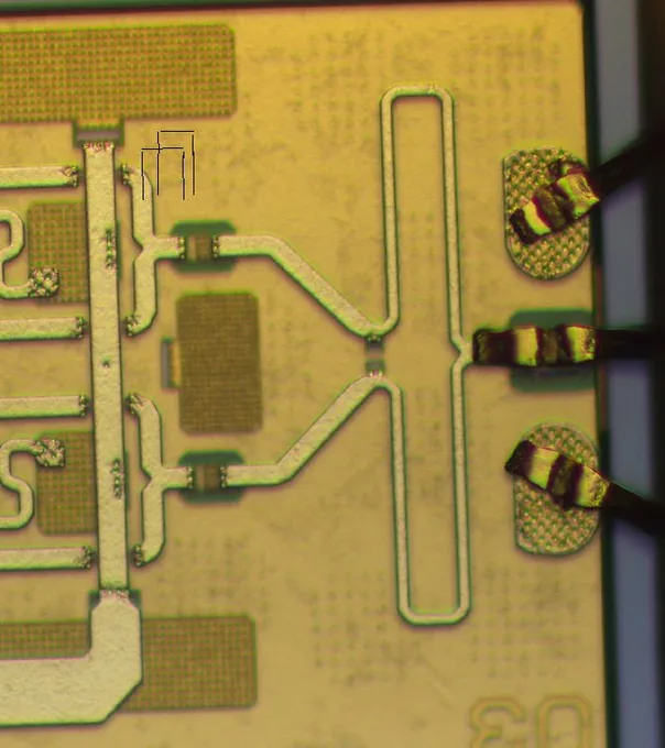
AlN, Rogers PTFE, low-loss substrate-matched attach
Ground-plane continuity, fluxless process
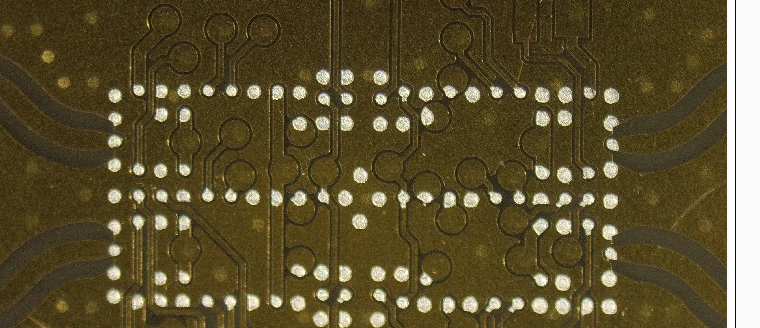
Sub-millimeter pitch capable
Full design rules, loss budgets, and build data available under NDA.
What we build for RF & mmWave
From eval board
to hermetic module.
RF eval boards, test vehicles, and production-intent modules – assembled around the signal path, not bolted on after it. The assembly choices that move your insertion loss happen here.
Every assembly choice that moves your insertion loss - flux-free reflow, die attach, and thin-film metallization - happens here, on US soil, for RF and mmWave programs.
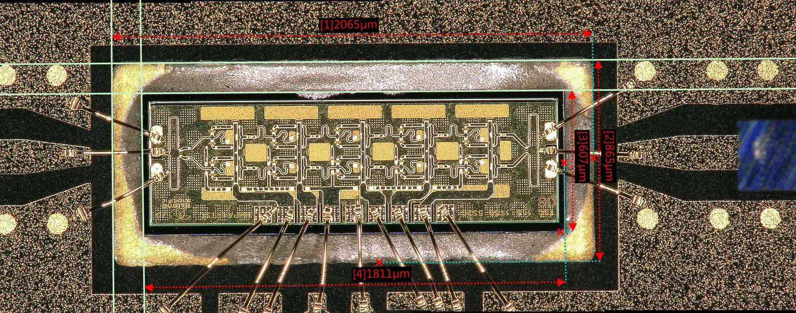
- 01GaN and GaAs die attach for power amplifiers, LNAs, and switches
- 02Antenna-in-package (AiP) and module integration for mmWave front ends
- 03Flip-chip and wire-bond interconnect tuned for low parasitics
- 04Fluxless, maskless assembly on AlN for clean, low-loss interfaces
- 05Hermetic packages for moisture-sensitive, reliability-critical RF
- 063D heterogeneous integration to shorten interconnect and stack function
Wafer 2″–12″ · die→substrate, die→wafer, die→PCB · advanced packaging across the stack.
Why it matters
At mmWave, the package
is part of the circuit.
Signal integrity
Flux residue is dielectric loss sitting on your trace. Fluxless, maskless assembly keeps the interface clean, so the loss you measure is the loss you designed – not contamination you have to chase.
Thermal management
GaN power amplifiers dump heat into the substrate. AlN moves it out fast and stays dimensionally stable, holding junction temperature down so RF performance and reliability hold together over life.
Yield you can trace
Every build is inspected and recorded – X-ray, 3D AOI, and sub-micron metrology. Yield is a number we can show you, with the data behind it, not a claim.
Get these three right and a tight loss budget closes on the first build instead of the third – that is the schedule and cost difference for an RF program.
The substrate is
a design choice.
AlN for thermal and low loss. Sapphire and quartz where the dielectric matters. Si for CMOS-compatible integration. We match the carrier to the band, the power, and the reliability target.
Thin-film metallization, controlled underfills, and qualified attach materials round out the stack. Material selection and the rules that go with it are part of the materials conversation – full detail under NDA.
How we engage
Coupon first. Then scale.
We start with a test vehicle or coupon that exercises the hard part of your build – the attach, the interconnect, the thermal path – and prove it against real metrology before anyone commits a full lot.
One engineering team carries the program from that first coupon through qualification and production-intent. Reliability and test – thermal cycling, screening, hermetic test, MIL-STD when the program calls for it – are built into the path, not bolted on at the end.
TYPICAL PATH
Process More.
Send us the RF build
that won't close its loss budget.
Request a capability brief for design rules, attach and interconnect detail, and build data under NDA – GaN, GaAs, AiP, and hermetic RF, assembled on US soil.
/ US-soil / traceable / MIL-STD
RF & mmWave FAQ
Engineer questions.
Do you assemble GaN and GaAs die for RF power?
Yes. We attach GaN and GaAs die for power amplifiers, LNAs, and switches, with the substrate and attach material chosen for the thermal and loss budget of the band you are working in.
Why fluxless, maskless assembly for RF?
Flux leaves residue, and residue is dielectric loss and a reliability risk on a high-frequency interface. Fluxless, maskless assembly keeps the interface clean, so insertion loss stays where you designed it.
Can you build antenna-in-package and mmWave modules?
Yes. We integrate antenna-in-package and mmWave front-end modules, combining flip-chip or wire-bond interconnect, low-loss substrates such as AlN, and hermetic packaging where the application requires it.
What do I get in a capability brief?
Relevant design rules, attach and interconnect detail, applicable materials, and build data for work like yours – shared under NDA. Send the build that has to close its loss budget and we will scope it engineer to engineer.