Capability / Materials
Materials we
already process.
Silicon, sapphire, quartz, AlN, polyimide, underfills, and thin-film metal stacks – characterized on real builds, not a datasheet. If your substrate is on this page, we have run a process on it.
/ Wafer 2in–12in / CMOS-compatible / US-soil
The material set
Substrates and stacks on the floor.
Each material below carries known process windows for dicing, deposition, attach, and inspection. Bring a new one and we will characterize it the same way – test vehicle, DOE, metrology.
Silicon, CMOS-compatible
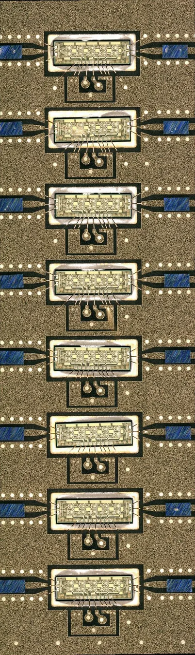
Device and interposer-grade wafers, 2in through 12in. Thinned die handling, TSV-ready, and back-end-of-line clean – the workhorse for logic, MEMS, and sensor builds.
Sapphire
Hard, optically clear, and thermally stable. UV-laser diced and singulated for photonics, optical windows, and high-reliability sensor packages where a brittle substrate has to come out clean.
Quartz / fused silica
Low-loss, low-CTE substrates for RF, timing, and optical work. Machined and metallized without chipping the edge that matters.
Aluminum nitride (AlN)
High thermal conductivity ceramic for power and RF carriers. Fluxless, maskless die attach demonstrated on 10+ RF boards at 100% yield – heat out, signal clean.
Polyimide & flex
Flexible dielectric for redistribution, flex circuits, and conformal sensor builds. Patterned and laser-processed where rigid substrates will not bend.
Underfills
Capillary and no-flow underfills qualified alongside flip-chip attach to manage thermomechanical stress across >900-bump packages without voiding.
Thin-film metallization
PVD/CVD/ALD metal stacks for pads, seed, RDL, and bond surfaces. Adhesion and barrier layers tuned to the attach and wire-bond step that follows.
Metals & technical ceramics
Lead frames, carriers, and ceramic substrates laser-cut, marked, and prepped for assembly – the parts that hold everything else together.
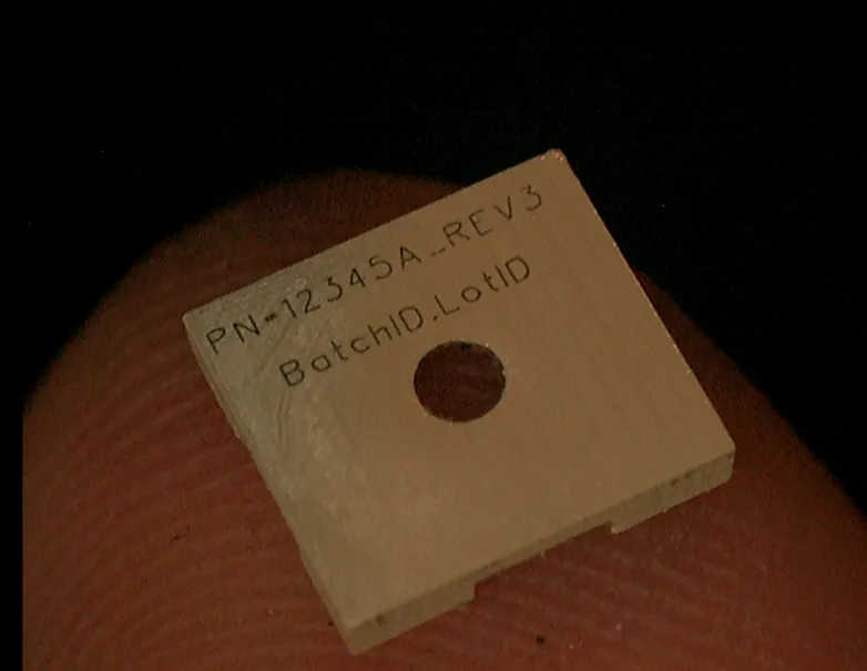
Detailed material design rules and process windows available under NDA.
Material → process
Pick the substrate. We will tell you the step.
Material choice drives the process. Here is where each one lands, with a link straight to the capability that runs it.
Why material fit matters
The substrate decides whether it survives.
A wrong material pairing does not fail on the bench. It fails at thermal cycle, at the RF corner, or two years into the field. We screen for that before the build, not after.
Pick the substrate for the physics, then let the process follow. We match coefficient of expansion, conductivity, and surface chemistry to the attach and metrology steps that come next.
Thermal
CTE mismatch and heat path drive solder fatigue and warpage. AlN and matched underfills move heat out and keep the joint intact through cycling.
RF / mmWave
Dielectric loss and surface roughness cost you at high frequency. Low-loss quartz and clean AlN carriers hold the signal where it counts.
Hermeticity
Sealing surfaces and bond-line integrity decide whether moisture stays out of a hermetic package. Material choice and metallization set the hermetic-test result.
Reliability
Adhesion, barrier layers, and clean edges survive screening and MIL-STD qualification. We validate with inspection and metrology on every build.
Proof, from real material builds
Si, sapphire, quartz, AlN, polyimide
Wafer handling range · CMOS-compatible silicon · thinned die
CMOS-compatible, no cross-contamination
Full material design rules, process windows, and build data available under NDA.
Where these materials ship
Built for the hard environments.
Aerospace and defense, medical and bio, RF and mmWave, advanced sensors – the programs where the substrate has to hold up. We process the material set those buyers actually qualify on.
How we engage
Bring the substrate. We bring the data.
- 01Tell us the material, geometry, and the step you need run
- 02We map it to an existing process window or build a test vehicle
- 03DOE and metrology confirm the window before production-intent
- 04Inspection, cross-section, and test validate every build
- 05Documented handoff – one engineering team, on US soil
No material is a mystery if you measure it.
If we have not run your exact stack, we characterize it the same way we characterize everything – with a test vehicle and real metrology, not a guess. Deeper specs are available under NDA.
Process More.
Tell us your substrate.
We will tell you the process.
Request a capability brief for material design rules, process windows, and build data under NDA. One engineering team, design review through volume.
/ US-soil / traceable / MIL-STD