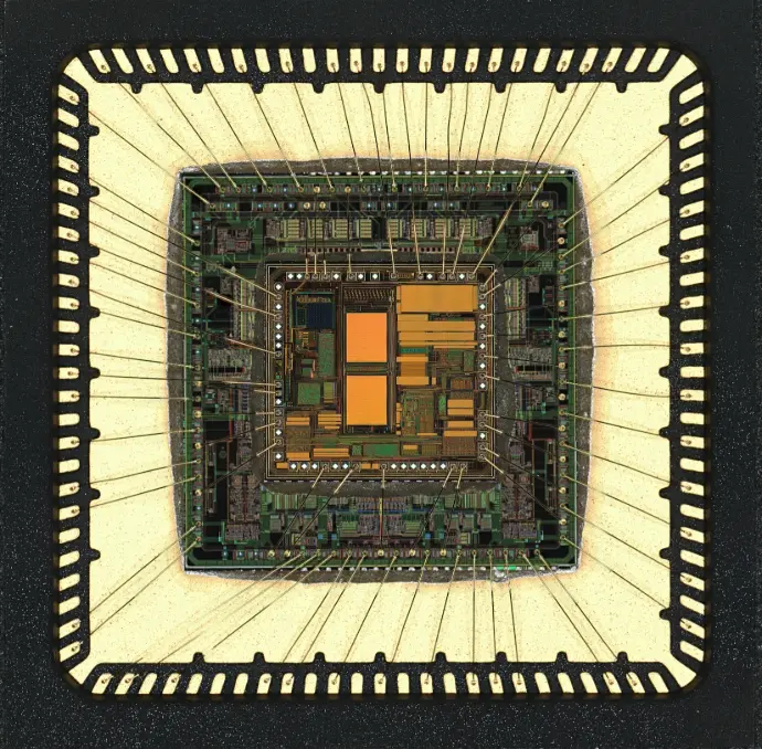
Advanced Packaging / 3D & HI
Many dies.
One package.
Chiplets, stacked die, and interposer modules – integrated into one qualified package. We attach, route, and stack heterogeneous parts from different processes and bring them up as a single working assembly, on US soil.
/ 2″–12″ / ±2.5µm @3σ placement / MIL-STD when required / US-soil
Integration is the product.
Monolithic scaling is slowing. The way forward is to split a system into the right chiplets – logic, memory, RF, sensors – each on its best process, then re-integrate them in a single package.
That re-integration is the hard part, and it is what we build. We combine die stacking, 2.5D interposer assembly, and 3D module construction so dies from different wafers and process nodes come up as one electrically and mechanically sound package – characterized with real metrology, not assumptions.
Integration menu
Five ways to combine dies.
01
Die stacking
Die-on-die and die-on-wafer stacks with controlled bond-line and overhang, for memory-on-logic and sensor-on-ASIC builds.
02
Interposer assembly
Silicon and organic interposers as the routing layer between chiplets – fine-pitch attach onto the carrier, then carrier to substrate.
03
2.5D & 3D
Side-by-side chiplets on a shared interposer (2.5D) and vertically stacked die through TSVs (3D) in one module.
04
Multi-die modules
Multi-chip modules mixing logic, RF, power, and sensing on a single carrier – one package, many functions.
05
Mixed-process integration
Parts from different nodes, foundries, and material systems – Si, AlN, sapphire – co-packaged with matched thermal and stress handling.
→
Not sure which?
Bring the system. We scope the partition and the package together at design review.
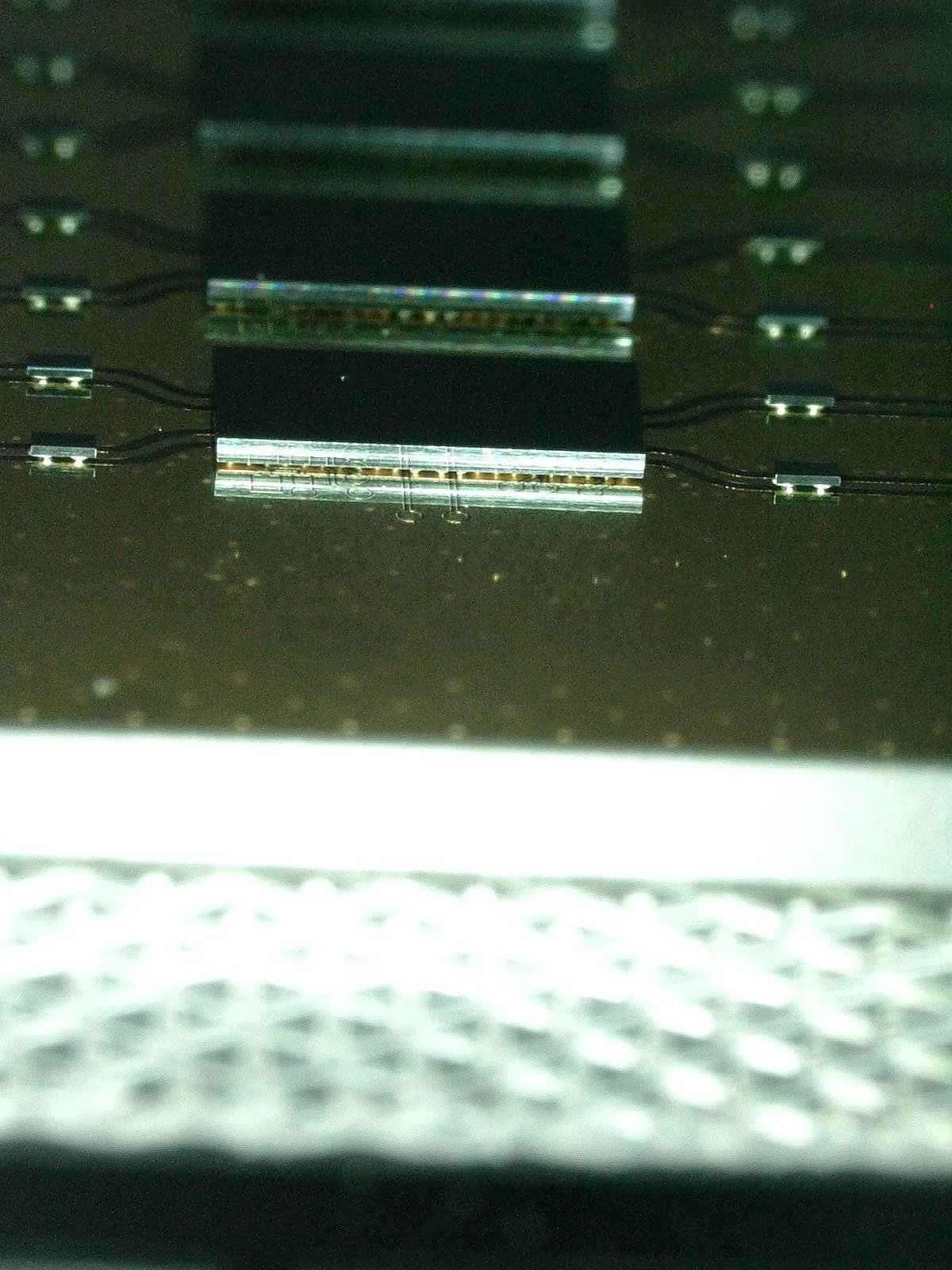
Request a brief →The wafer-level under-layer
3D starts below the die.
Heterogeneous integration only works when the interconnect underneath it is built right. The vertical and lateral paths between dies come from wafer-level process.
We build the through-silicon vias, redistribution layers, and interposers that carry signal and power between stacked and side-by-side dies – then assemble onto them in the same shop, so the hand-off never crosses a vendor boundary.
Stack shown top-to-bottom. Layer counts, pitches, and via geometry are scoped per build – detail under NDA.
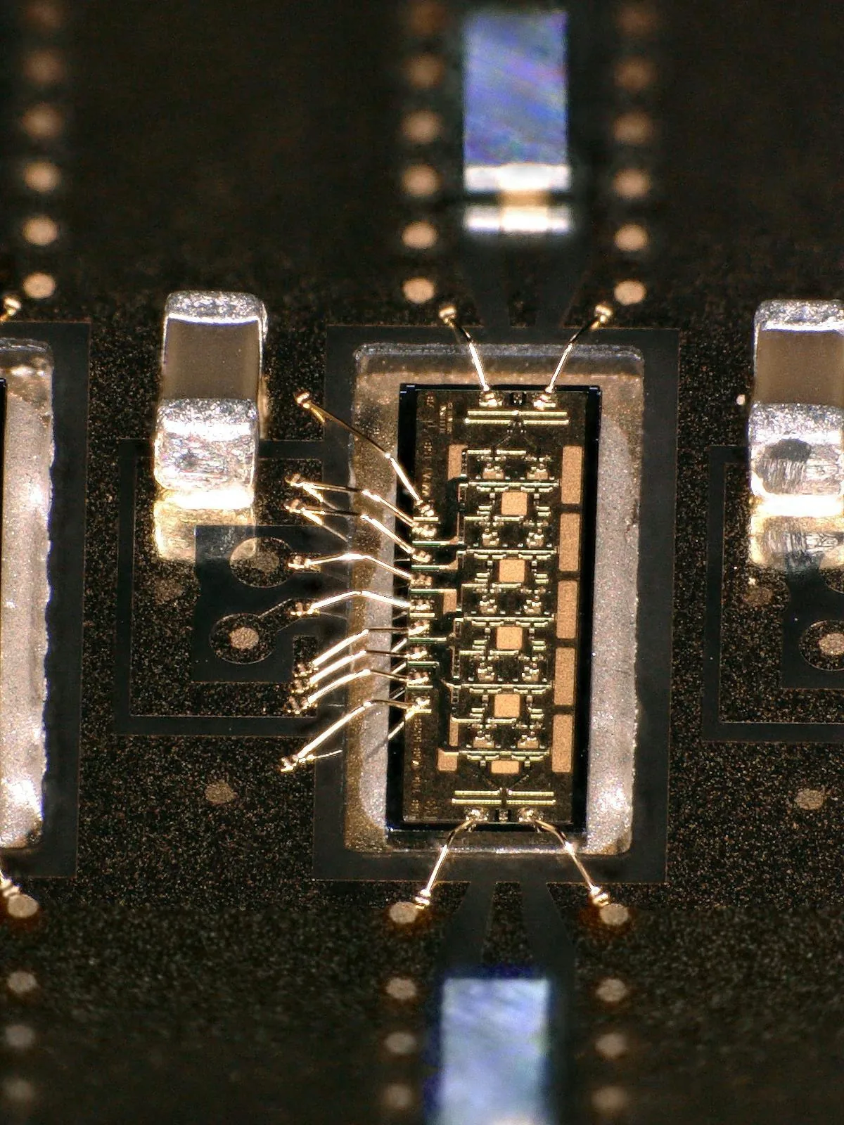
Attach & interconnect, under the hood
How the dies actually connect.
- 01Flip-chip attach – C4, C2, and Au-stud, with capillary and no-flow underfill, down to fine pitch on interposers and substrates.
- 02Precision die bonding – ±2.5µm @3σ placement on BESI Datacon and Tresky platforms, die→wafer, die, substrate, or PCB.
- 03Wire and ribbon bond – where stacked tiers or mixed dies still need a wired path.
- 04Underfill & encapsulation – matched to the stack's thermal and mechanical profile to control stress across tiers.
Proof, from real builds
Heterogeneous Si, GaAs, InP, SiC stacks
TSV, RDL, interposer routing
MIL-STD screening available
Full design rules, stack-up detail, and build data available under NDA.
See inside the stack
A 3D package hides its defects.
Once dies are stacked, the joints you most need to trust are buried. We verify them without taking the part apart.
X-ray (Creative Electron) reads voids, bridges, and bump integrity through the stack. 3D AOI checks placement and bond-line. SEM and cross-section confirm interface quality on first articles, and sub-micron metrology ties every tier back to the design intent – the data engine behind every qualified module.
Where it fits
Built for the hard programs.
Aerospace & Defense
SWaP-driven modules, MIL-STD qualification, US-soil supply.
Medical & Bio
Miniaturized multi-die sensors and implant-class assemblies.
RF & mmWave
Mixed-process RF front-ends co-packaged on low-loss carriers.
Advanced Sensors
Sensor-on-ASIC stacks where pitch and stress decide yield.
Common questions
Before you send a stack-up.
Do you do true 3D stacking with TSVs, or only 2.5D side-by-side?
Both. We assemble side-by-side chiplets on a shared interposer (2.5D) and vertically stacked die through TSVs (3D), and we build the TSV, RDL, and interposer layers in-house so the wafer-level and assembly steps stay under one roof.
Can you integrate dies from different foundries and process nodes?
Yes – mixed-process integration is the point. We co-package parts from different nodes, foundries, and material systems (Si, AlN, sapphire) with matched thermal and stress handling so the heterogeneous stack behaves as one part.
What placement accuracy can you hold on interposer attach?
±2.5µm at 3σ on BESI Datacon and Tresky platforms, across die→wafer, die, substrate, and PCB. Finer-pitch design rules are available under NDA.
How do you verify joints buried inside a stack?
X-ray (Creative Electron) for voids, bridges, and bump integrity through the stack; 3D AOI for placement and bond-line; SEM and cross-section on first articles; sub-micron metrology to tie each tier to design intent.
Is this done on US soil?
Yes. Wafer-level build and assembly run domestically, with MIL-STD qualification when the program requires it.
Process More.
Bring us the dies.
We'll bring back the package.
From chiplet partition through stacked, qualified hardware – one engineering team, on US soil. Request a capability brief for design rules, stack-up detail, and build data under NDA.
/ US-soil / traceable / MIL-STD