About
Engineers who
develop the process.
Heisler Semiconductor is a US-based, engineering-led advanced packaging team. We take hard assembly and wafer-level processes from design review to qualified volume – data-driven, AI-native, and built on US soil.
/ Maryland lab / US-soil / NDA-first
Are we real? Read the build data.
Design, firmware, packaging & test under one roof
Domestic, MIL-STD when required
Built from real hardware programs
DOE & SPC on every build
Aggregate results from real Heisler builds. Full design rules, process detail, and build data available under NDA.
One team, design
review to volume.
We are a packaging and process partner for companies building hard hardware – the kind where a die has to land within microns, survive thermal cycling, and pass on the first qualified lot.
Our work spans die attach, wire bond, and flip chip; wafer-level processing and interposers; laser micromachining; and the inspection and metrology that proves every step. We do not hand you off between vendors and recipes – the same engineers who scope the job own it through qualification. Explore the full advanced packaging capability map, see how our engineering & AI approach cuts iterations, and review the domestic supply-chain management that keeps a program on US soil end to end.
How we work
Rigor you can audit.
We treat process development as an engineering problem, not trial and error. Define the objective, build a test vehicle, run the DOE, validate with real metrology, document what we learned.
Data decides; an engineer signs off. Every adjustment stays traceable and tied to manufacturability and reliability – so the second lot looks like the first.
- 01DOE-driven development – designed experiments, not guesses, to find the stable window fast
- 02SPC & data-driven control – process, inspection, metrology, and test data aggregated per build
- 03AI-assisted iteration reduction – AI surfaces drift and correlations; engineers own the call
- 04US soil, start to finish – development and build stay domestic
- 05NDA-first – your design rules, materials, and yields stay yours; deep detail moves under NDA
Fewer trial-and-error iterations · faster convergence on stable process windows · documented change control before production-intent.
Where we are
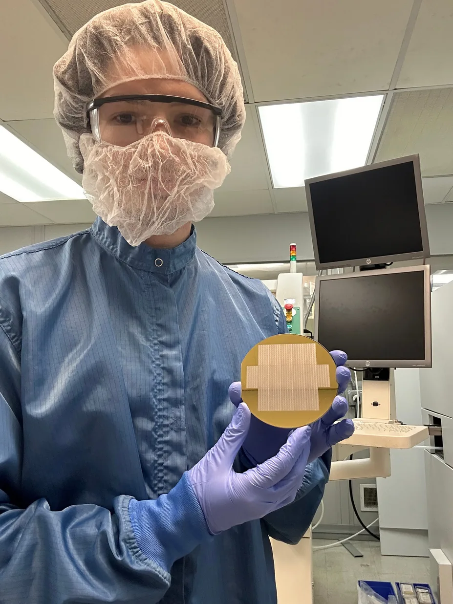
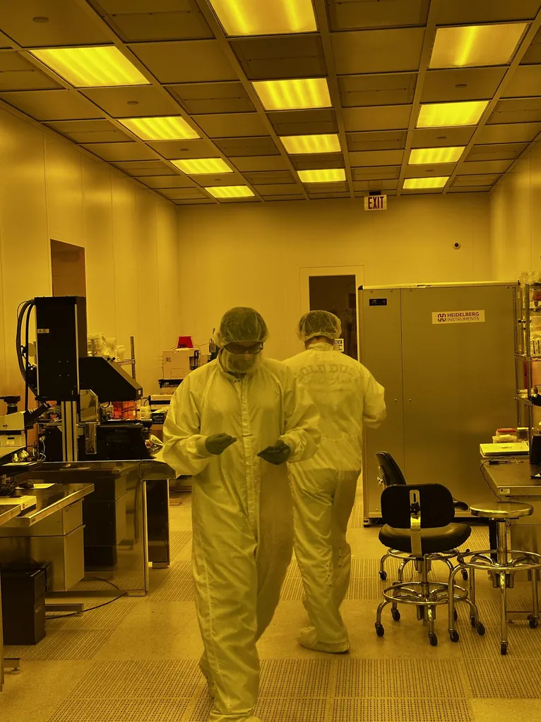
A real lab in Maryland.
Our process and assembly lab sits in Halethorpe, Maryland – not an offshore floor, not a broker. You can visit, review a build, and watch the data come off the line.
We run a domestic supply chain: US sourcing, vetted vendor coordination, and structured handoffs that keep sensitive programs inside US borders. That matters for aerospace & defense, medical, and RF work where provenance and domestic sourcing are not optional.
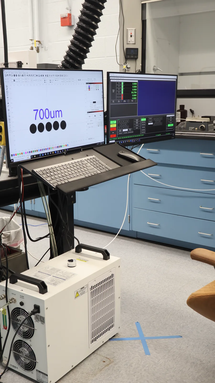
Tooling we run
Named equipment. Documented results.
The tool list is the easy part. The value is the recipe we develop on it.
See the full toolset and process detail in a capability brief, or talk to sales about your build.
Common questions
Before you reach out.
Where is Heisler Semiconductor located?
Our process and assembly lab is in Halethorpe, Maryland (1448 S Rolling Rd, Suite 021, Halethorpe, MD 21227). All development and build work is performed on US soil with a domestic supply chain.
What does Heisler actually do?
Advanced packaging and process development: die attach, wire bond, and flip chip; wafer-level processing and interposers; laser micromachining; and the inspection and metrology that qualifies it. One engineering team owns the work from design review to qualified volume.
What makes the approach AI-native?
We aggregate process, inspection, metrology, and test data across every build and use AI as a decision-support layer to surface drift and correlations – reducing trial-and-error iterations. An engineer signs off on every change, and the trail stays traceable.
Is the work US-based?
Yes. Heisler Semiconductor LLC operates in Maryland with a domestic supply chain, supporting aerospace & defense, medical, RF/mmWave, and advanced-sensor programs where provenance and domestic sourcing matter.
How do I see real process detail?
Design rules, full process detail, and build data move under NDA. Request a capability brief or talk to sales at sales@heislersemiconductor.com and we will scope your build.
Process More.
Real engineers.
Real lab. Real data.
One US-based team, design review through volume. Request a capability brief for design rules, full process detail, and build data under NDA.
/ US-soil / NDA-first / Maryland lab