Resources
Briefs, on request.
Design rules, process windows, and real build data — written engineer-to-engineer. Tell us your application and we send the brief that maps to it. Depth in exchange for a conversation.
/ NDA-grade detail / US-soil / MIL-STD when required
Available briefs
Pick the one that matches your build.
Each brief is scoped to a capability. Request it and a process engineer returns the relevant design rules, process windows, and case data under NDA.
Inside a brief
Not a datasheet. A build record.
A capability brief is what an engineer needs to decide whether to hand us the work. It is specific, it is referenced to real builds, and it goes under NDA so we can talk numbers instead of adjectives.
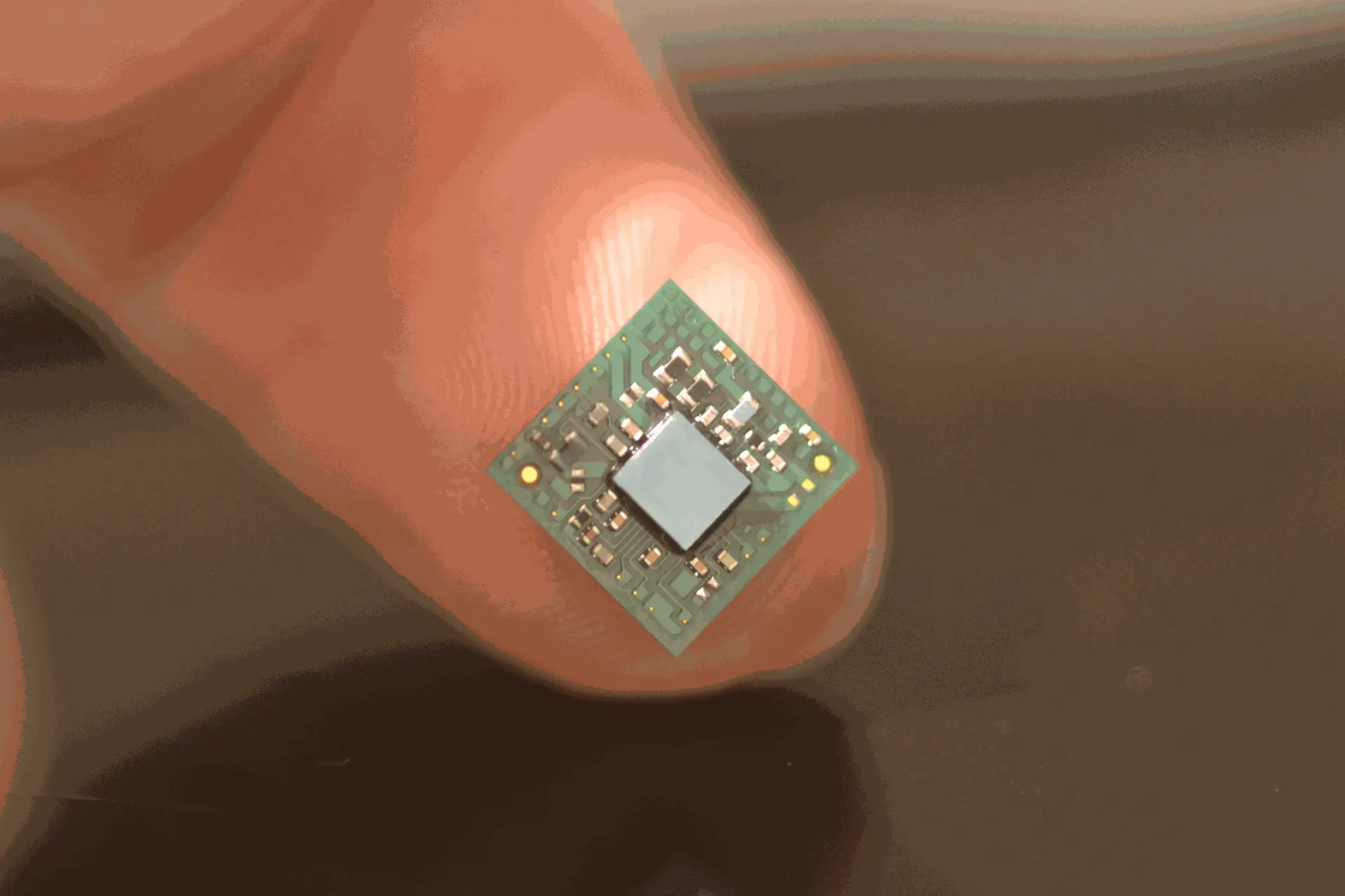
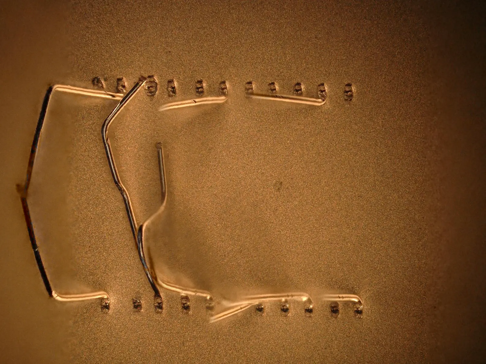
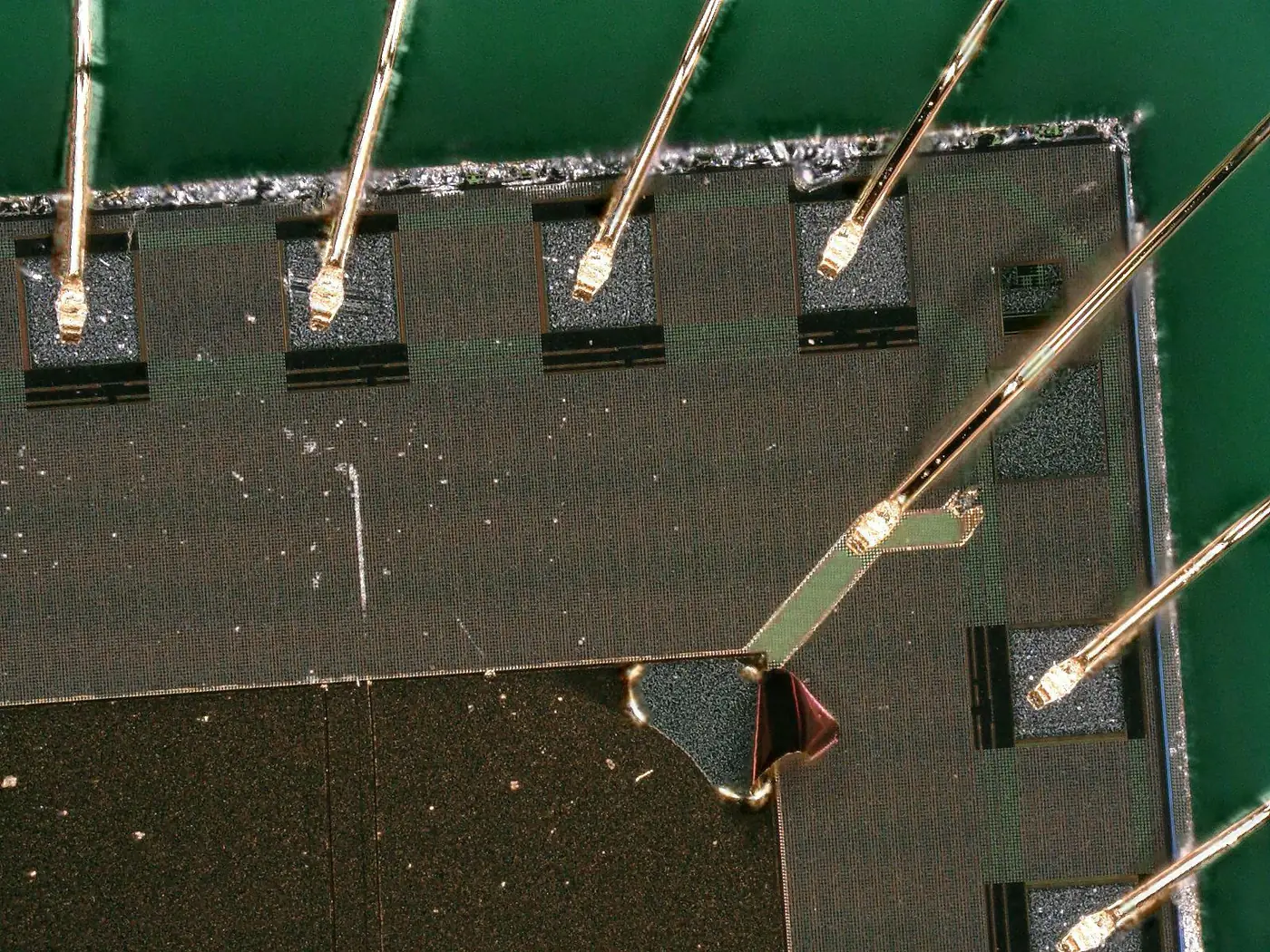
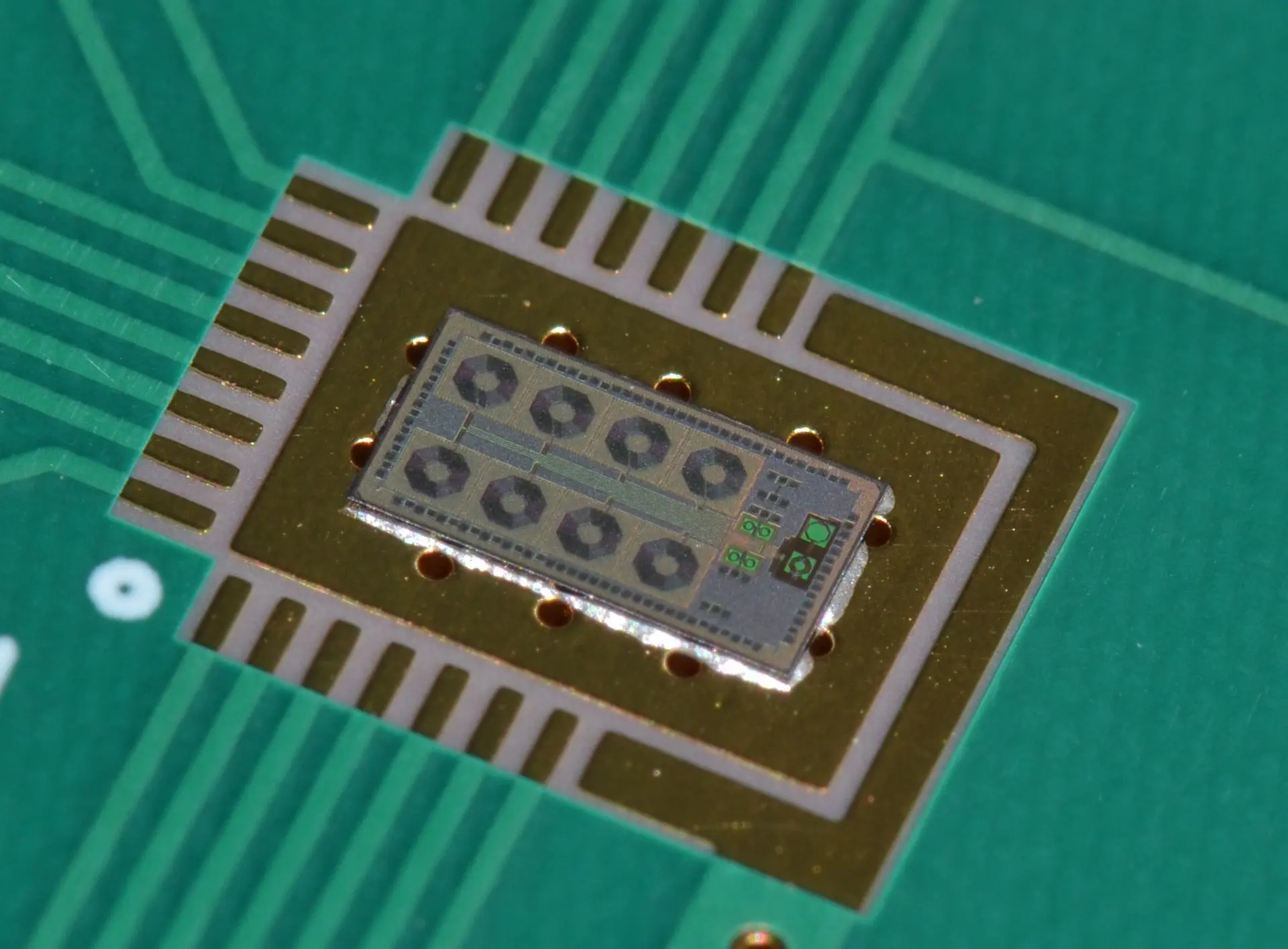
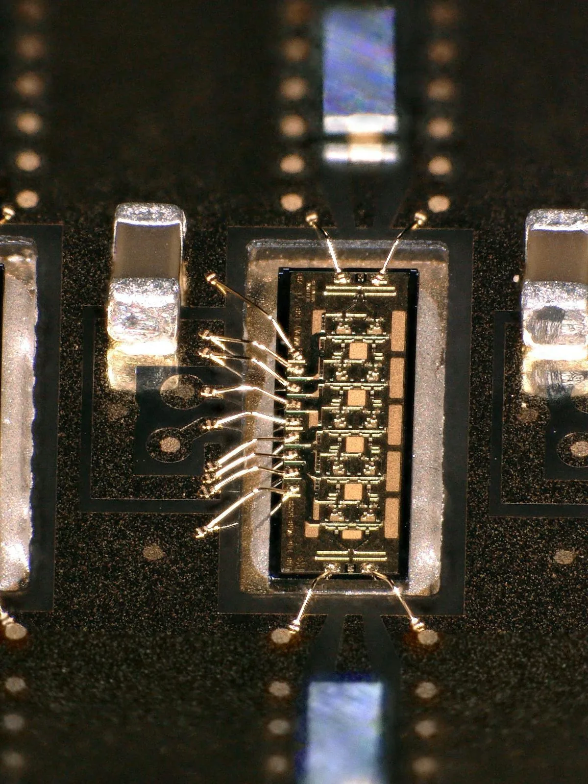
Pitch, bump, and pad geometry; substrate and material limits; placement tolerance; what we hold and where the edges are.
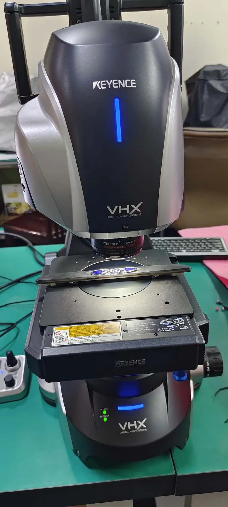
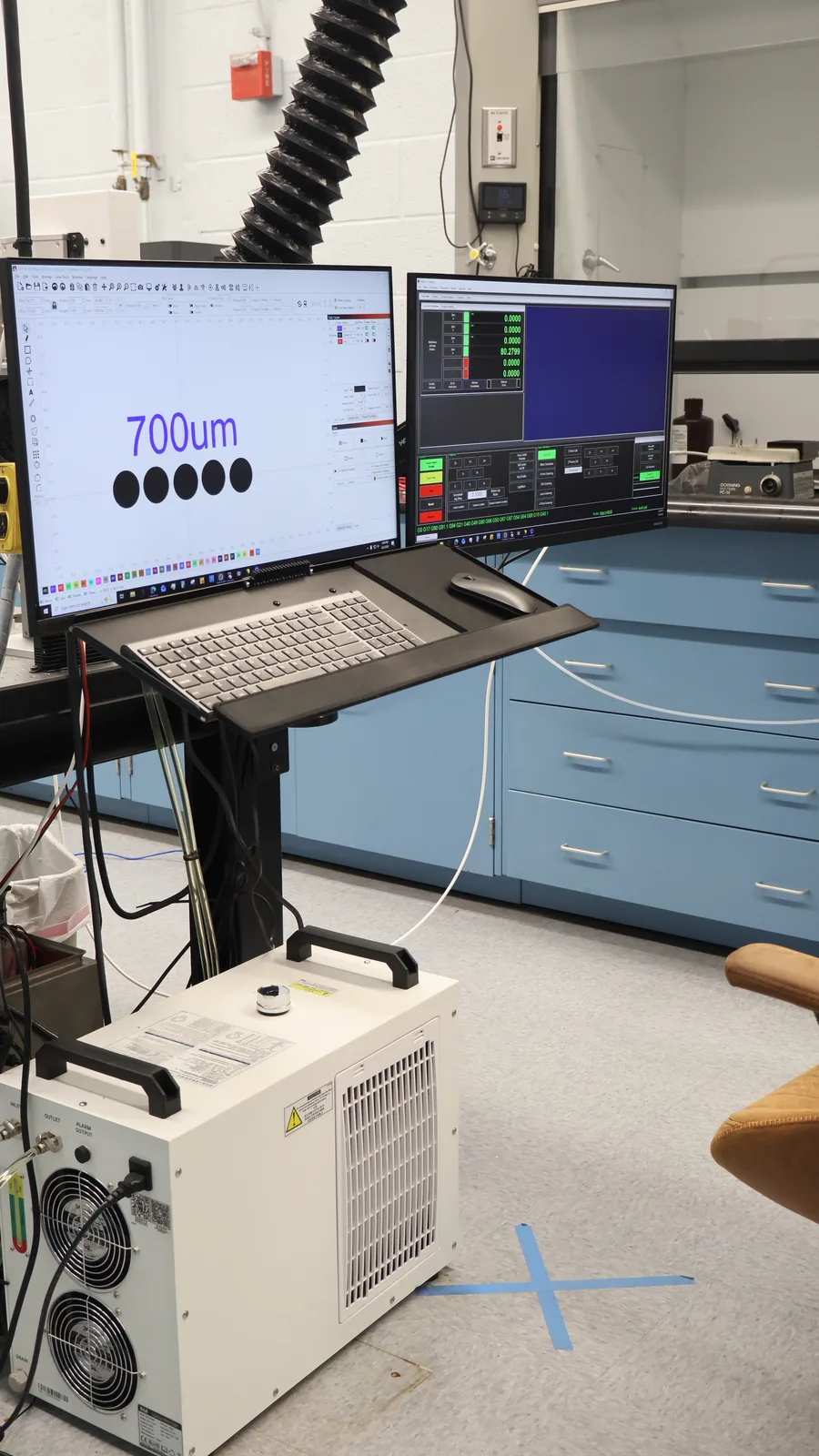
Validated parameter ranges from DOE and SPC — the stable region, not a single demo point, with the metrology that confirms it.
Yield, defect modes, and reliability results from comparable builds — so you scope against evidence, not a brochure.
Full design rules, process detail, and build data are shared under NDA.
Request a capability brief — an engineer will scope your build.
FAQ
Answers before you ask.
What materials do you process?
Silicon (CMOS-compatible), sapphire, quartz, AlN, polyimide, thin-film metallization, and underfills. Laser work runs across Si, sapphire, ceramics, metals, and polymers. Wafer sizes 2″ through 12″.
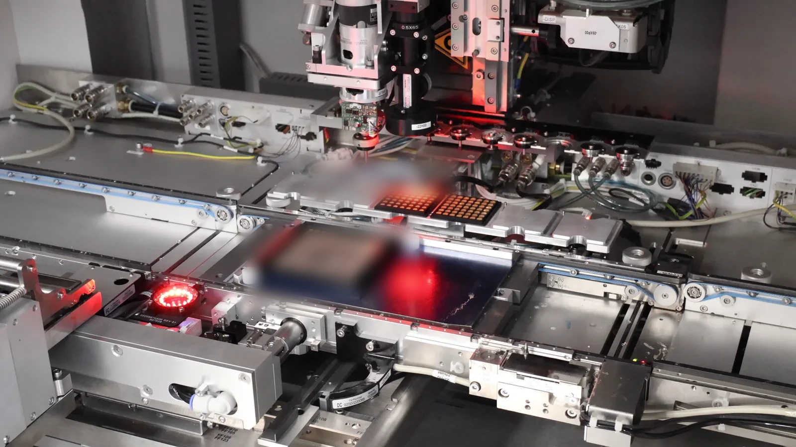
What placement accuracy can you hold?
±2.5µm @3σ on BESI Datacon and Tresky platforms — die to wafer, die, substrate, or PCB. Documented builds include a >900-bump flip-chip package at 100% yield. Tighter rules go under NDA.
Which industries do you serve?
Aerospace & defense, medical & bio, RF/mmWave, and advanced sensors. Programs run SPC-controlled, MIL-STD when required.
Is the work done on US soil?
Yes. Engineering, assembly, inspection, and test are performed in the United States with domestic sourcing — one engineering team from design review through volume.
How do I get a brief?
Use the contact form with your application and target specs. A process engineer scopes it and returns the relevant design rules, process windows, and case data under NDA.
Why request one
Scope faster. Guess less.
A brief turns a vague feasibility question into a referenced answer. You see whether your geometry, materials, and tolerances sit inside our proven window before you commit a tapeout or a build slot.
- 01Real design rules and tolerances, not marketing ranges
- 02Process windows validated by DOE, SPC, and metrology
- 03Case data from comparable, documented builds
- 04A direct line to the engineer who would run your work
Related pillars: Flip Chip · Advanced Packaging · Wafer-Level · Laser · Inspection & Metrology.
Process More.
Tell us the build.
We’ll send the brief.
One form. A process engineer reads it and returns design rules, process windows, and build data matched to your application — under NDA.
/ US-soil / traceable / MIL-STD