Advanced Packaging
Bond, attach, integrate.
Die attach, flip chip, wire bond, hermetic, and 3D heterogeneous integration — from R&D through production-intent, on US soil. One engineering team owns the process from first build to repeatable yield.
/ Placement ±2.5µm @ 3σ / MIL-STD when required / US-soil
What we do
Five attach and interconnect families, under one roof.
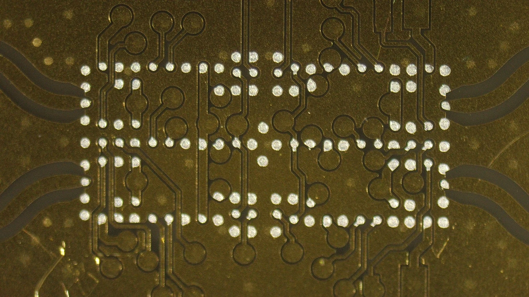
Wafer handling 2″ to 12″. Placement to ±2.5µm at 3σ on BESI Datacon and Tresky platforms. The recipe set covers most die-to-substrate problems — the rest we develop.
Hermetic sealing · fluxless / vacuum reflow · mixed-die stacks · panel-level builds. Full process windows and design rules available under NDA.
- 01Die attach & dispense — automated dispense, dip & stamp; conductive and non-conductive adhesives
- 02Bonding methods — epoxies, fluxless and vacuum reflow, thermocompression, ultrasonic, ACA/ICA
- 03Flip chip — C4 solder ball, C2 Cu-pillar, Au stud; capillary and no-flow underfill
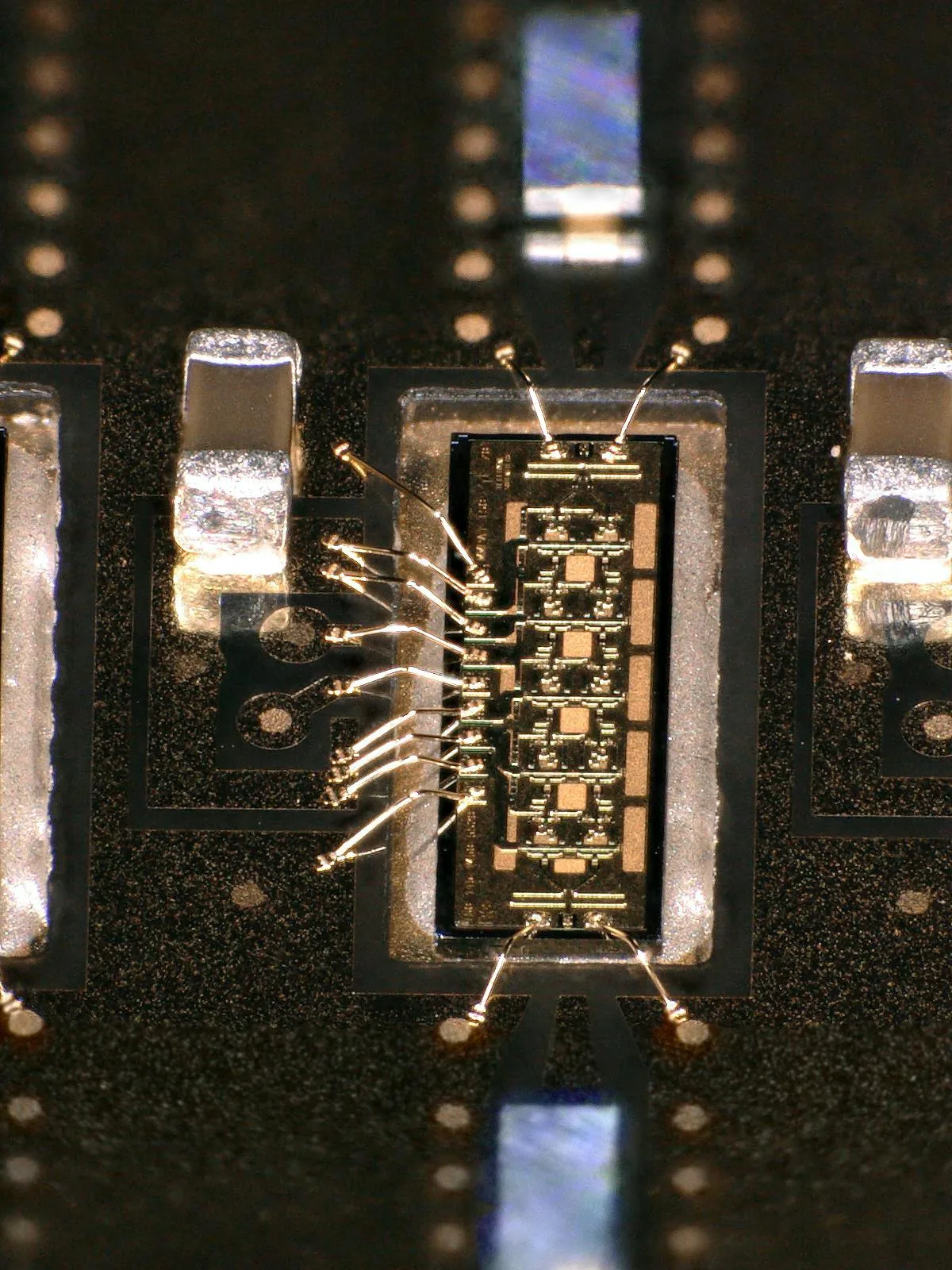
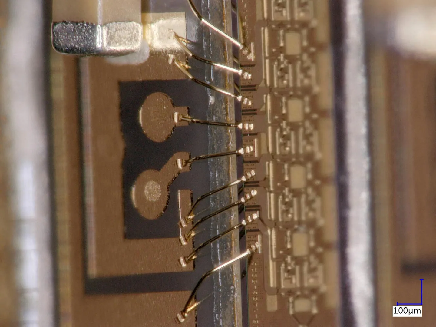
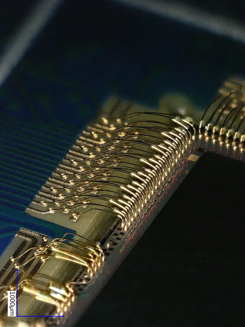
- 04Wire bond — ball and wedge, fine pitch
- 053D heterogeneous integration — die-to-wafer, die-to-die, die-to-substrate, die-to-PCB
The first build is easy. The hundredth is the job.
A package that works once tells you nothing. We develop the attach process so it holds across lots — controlled placement, controlled bondline, controlled void rate — then prove it before you commit to volume.
New geometries break old recipes: thinner die warp, finer pitch shorts, mixed-CTE stacks crack on the first thermal cycle. We treat each as an engineering problem — define the objective, build a test vehicle, run the AI-assisted DOE, validate with real metrology — so the failure mode shows up on a coupon, not in your field return.
Materials & applications
Hard substrates, fine pitch, high reliability.
Silicon, sapphire, AlN, and polyimide; conductive and non-conductive adhesives and underfills. Built for work that has to survive thermal cycling and screening.
Aerospace
& Defense
Hermetic · traceable · US-soil
Medical
& Bio
MEMS · sensors · panel-level
RF /
mmWave
Fine-pitch · Cu-pillar · multi-die
Advanced
Sensors
3D stacks · mixed-die · underfill
Proof, from real builds
Flip-chip bump families: C4, C2, Au-stud, capillary & no-flow underfill
Die-to-wafer, die-to-substrate, die-to-PCB attach
Placement accuracy @ 3σ · BESI Datacon · Tresky
Full design rules, process windows, and build data available under NDA.
How we qualify
Every build leaves evidence.
Qualification to MIL-STD or your spec — bond integrity verified, not assumed.
We close each process with metrology and reliability data, then document the window and change control so the result transfers cleanly to production-intent. Cross-section and x-ray detail lives with inspection & metrology; dicing and singulation with laser micromachining; RDL and TSV with wafer-level.
Process More.
Bring us the package
that won't yield yet.
One team, design review through volume. Request a capability brief for design rules, full process detail, and build data under NDA.
/ US-soil / traceable / MIL-STD