Wafer-Level Processing
Wafer in. Interposer out.
Wafer-level patterning, vias, deposition, etch, CMP, and RDL on one floor — so you iterate interposers and test vehicles in days, not a full-fab queue.
/ Maskless & direct-write / Si · sapphire · quartz · compound / TSV & RDL / US-soil
What we run
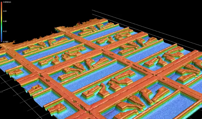
The wafer-level stack, end to end.
Every step that turns a blank wafer into a routed interposer or test vehicle, under one roof — no shuttle between vendors, no lost weeks at each handoff.
- 01Direct-write lithography & maskless patterning — no mask set, no NRE wait between design spins
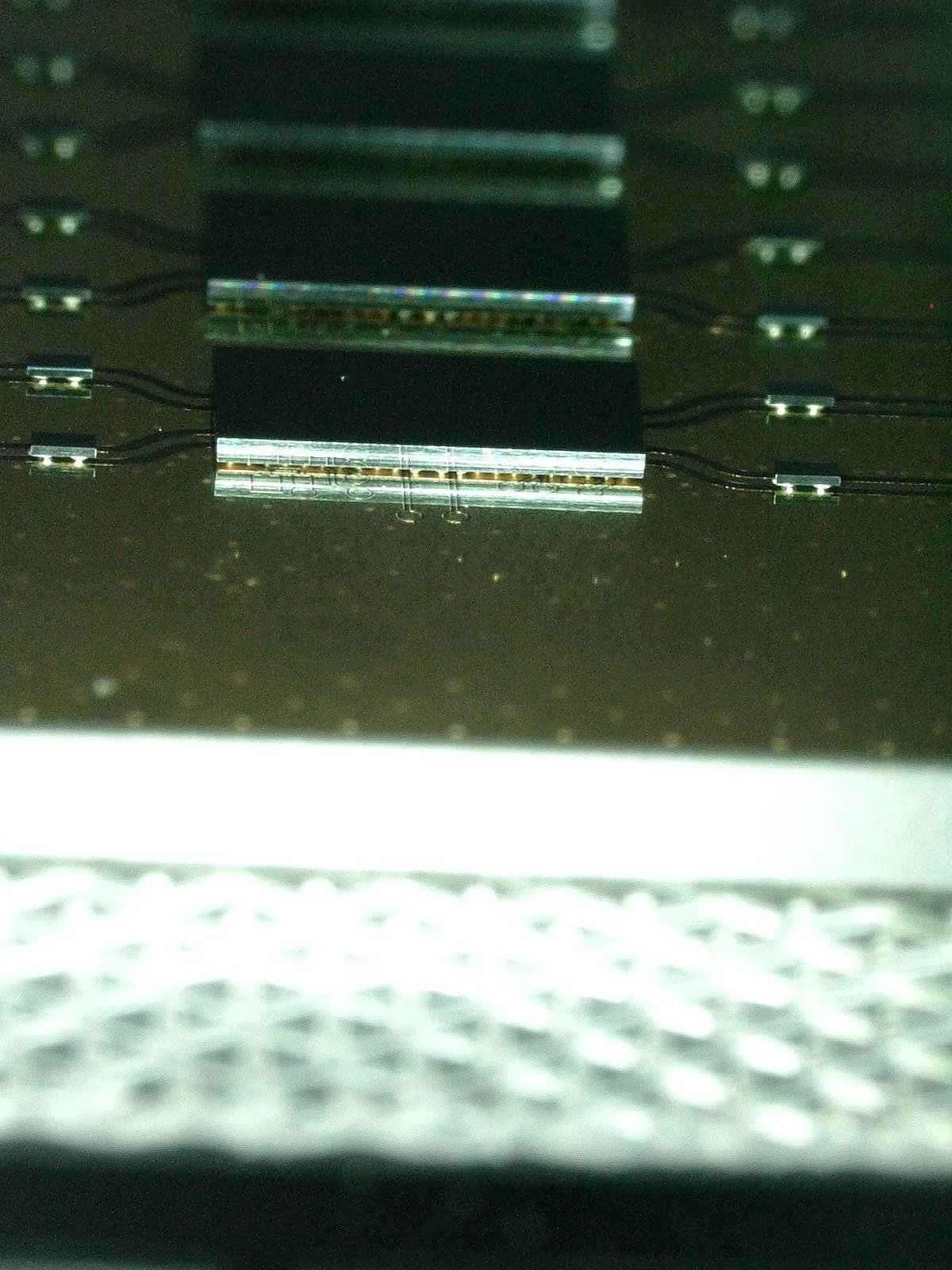
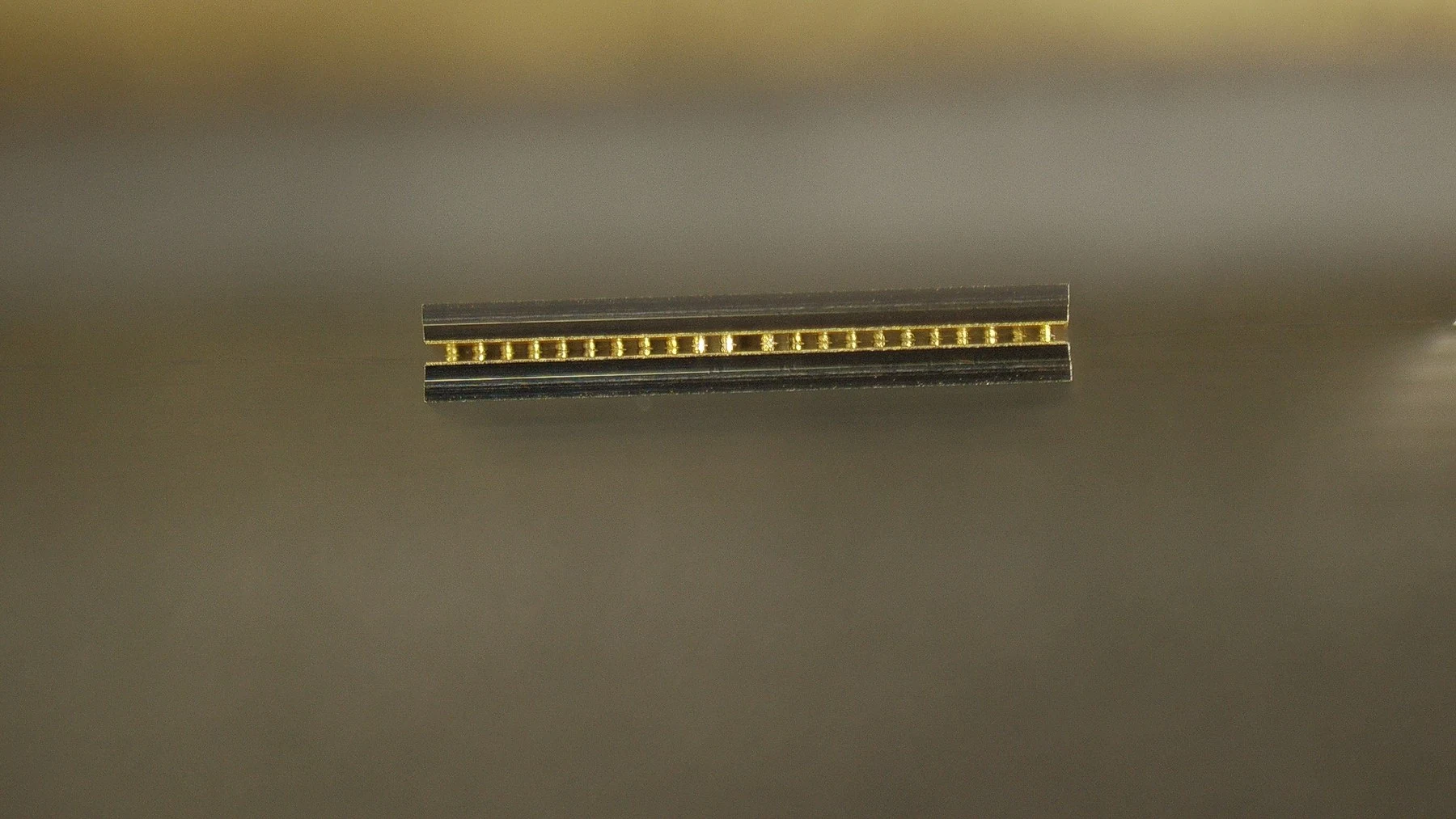
- 02Via formation, TSV and non-TSV — through-silicon and blind/buried vias for vertical interconnect
- 03Deposition — PVD, CVD, and ALD for seed, barrier, dielectric, and conformal films
- 04Etch — plasma, gas-phase, and wet chemistries for features, release, and via reveal
- 05Grinding & CMP — thinning and planarization to target thickness and surface finish
- 06RDL — redistribution routing to fan signals out to package-level pitch
Step-level recipes, film stacks, and design rules shared under NDA.
A full fab move-in to prove one idea?
Most wafer-level work stalls because each step lives at a different vendor. A litho spin waits on a mask house; a TSV etch waits in someone else's queue. Weeks evaporate between steps, not inside them.
We hold the whole flow in one place, so a design change closes in a single pass instead of a round-trip. Maskless patterning kills the mask-set wait on every spin. You get an interposer or test vehicle back fast enough to actually iterate on it — and the process that built it is documented, not improvised.
Substrates & targets
Wide material set. Hard targets.
Materials
Silicon
intrinsic & CMOS-compatible
Sapphire
hard, optically clear
Quartz /
fused silica
low-loss, RF & photonic
Compound
III–V & wide-bandgap
Applications
- 01Silicon interposers — 2.5D routing between die
- 02TSV test vehicles — via and stack qualification
- 03WLP & fan-out — wafer- and panel-level packaging
- 04Micro-fluidics, sensors & RF — etched channels, MEMS, low-loss passives
Substrate handling limits, thickness windows, and feature minimums confirmed against your design under NDA.
Proof
Process flows shared under NDA.
How we engage
Start with a test vehicle. Scale what works.
Send the structure you need built and the constraint you're fighting. We scope the flow, run a first wafer or test vehicle, and measure it before anyone talks volume.
One engineering team owns the wafer from patterning through RDL, so the result is traceable and repeatable — risk gets retired on the first build, not discovered at scale-up.
More capability
Where wafer-level connects.
/ Advanced Packaging / Laser Micromachining / Inspection & Metrology / Engineering & AI
Process More.
Bring us the wafer
that needs a faster loop.
One team, patterning through RDL. Request a capability brief for substrate limits, film stacks, design rules, and full process detail under NDA.
/ US-soil / Maskless / TSV & RDL