Advanced Packaging / RF & mmWave
RF packaging
without the flux.
Fluxless, maskless RF and mmWave assembly on AlN and thin-film substrates. No post-attach clean, no residue on your launch – the geometry you designed is the geometry we build.
/ AlN & thin-film / fluxless & maskless / ITAR-aware / US-soil
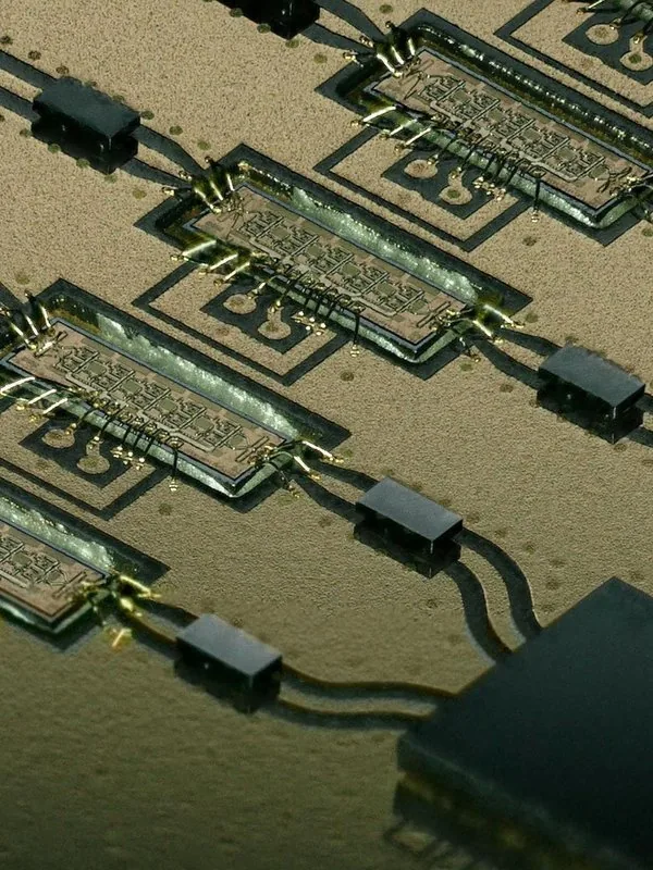
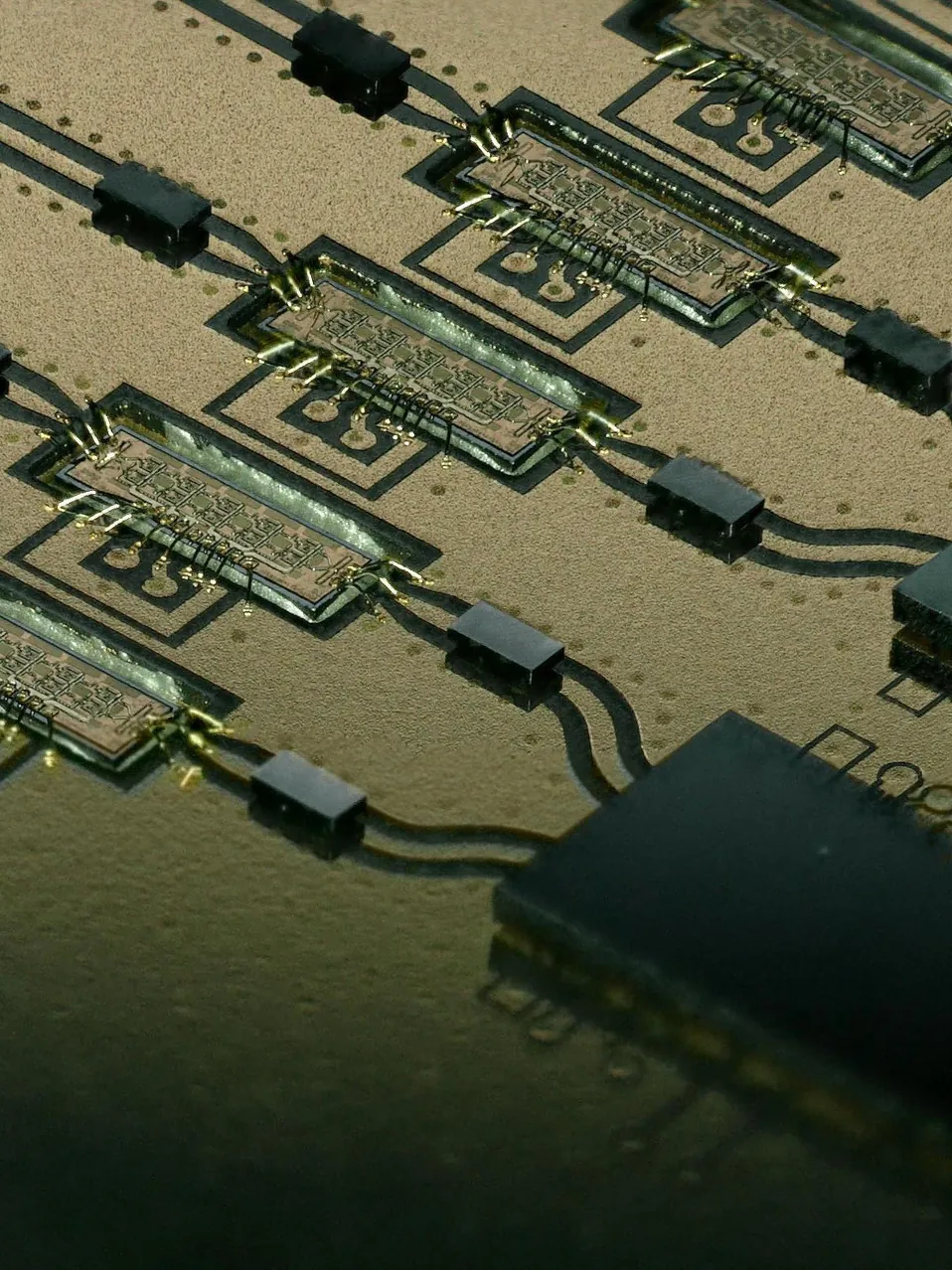
Proof, from real RF builds
RF boards on AlN · fluxless, maskless · 100% yield
Fluxless, maskless — no post-attach clean
AlN, Rogers, PTFE substrate-qualified
Full RF design rules, process detail, and build data available under NDA.
RF & mmWave capability
Built for high frequency.
RF and mmWave devices punish process noise. We build the assembly around the things that move S-parameters – substrate, interconnect length, metallization, and contamination – not around a generic die-attach recipe.
One engineering team owns the build from substrate prep through inspection and metrology, so every choice traces back to RF performance and reliability.
- 01AlN and thin-film substrates – low-loss, high thermal conductivity, controlled impedance
- 02Fluxless, maskless assembly – no residue, no post-attach clean
- 03Flip chip for RF – shortest, most repeatable interconnect at mmWave
- 04Short-loop wire bond where the device or layout calls for it
- 05Thin-film metallization for tight line-edge definition and ground integrity
- 06RF eval boards and test vehicles to characterize before you commit a module
Wafer 2″–12″ · die→substrate, die→PCB · inspection & metrology in-house.
Flux is residue.
Residue is loss.
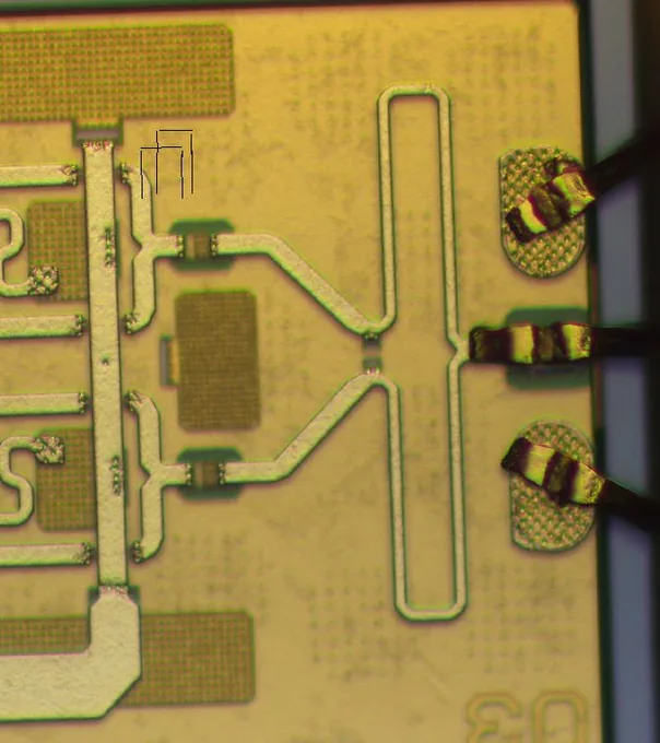
At mmWave, the dielectric a few microns above your transmission line is part of the circuit. Flux residue and the aggressive clean that chases it leave films and ionic contamination that shift impedance, add insertion loss, and seed long-term failures.
Fluxless, maskless assembly deletes that variable. There is no clean step to validate, no residue under a flip-chip die you can never inspect again, and no mask artifact on the launch. The result is a build that matches the model – repeatably – which is the only way an RF process scales past the first coupon.
Predictable impedance
No residual dielectric film changing the line you designed. The launch and transition behave the way the EM model says they should.
Lower insertion loss
Clean metal interfaces and tight thin-film geometry keep loss down where every tenth of a dB counts – at the top of the band.
Reliability you can defend
No ionic residue trapped under die or wire. Fewer failure modes to screen, and a cleaner story for qualification and field life.
Materials
The substrate is the circuit.
AlN is our default for RF power and mmWave because it pulls heat out while holding a low-loss, stable dielectric. We also run sapphire, quartz, and Si where the device wants them, with thin-film metallization sized to the frequency.
Choosing the substrate and metal stack is an RF decision, not a logistics one. See the full materials capability for what we build on and how we metallize it.
Where this fits
RF, mmWave, and defense.
How we engage
Coupon first. Then scale.
One team, design review through volume.
We retire the RF risk on a coupon before it costs you a module spin – on US soil, with the inspection and metrology data to prove the build. Related: flip chip and the full advanced packaging line.
RF packaging FAQ
Engineer questions.
Why does fluxless assembly matter for RF performance?
Flux residue and post-attach cleaning leave ionic contamination and films that change impedance, raise insertion loss, and risk long-term reliability at high frequency. A fluxless, maskless process removes the clean step, so the launch and transmission-line geometry you designed is what gets built.
Why AlN substrates for RF and mmWave?
AlN pairs high thermal conductivity with a low-loss, stable dielectric – it pulls heat from RF power devices while holding controlled-impedance lines tight. With thin-film metallization you get the line-edge definition and ground integrity mmWave modules need.
Flip chip or wire bond for RF?
We pick the interconnect to the frequency and parasitic budget: flip chip for the shortest, most repeatable interconnect at mmWave; short-loop wire bond where the device or layout calls for it. Both run in one shop alongside inspection and metrology.
Can you build RF eval boards and test vehicles?
Yes – on AlN and thin-film substrates, so you can characterize a launch, a transition, or a die before committing to a full module build. Full design rules and process detail are available under NDA.
Process More.
Send us the RF build
that won’t close its loss budget.
Fluxless, maskless RF and mmWave assembly on AlN, US-soil. Request a capability brief for design rules, full process detail, and build data under NDA.
/ US-soil / ITAR-aware / MIL-STD