Overview
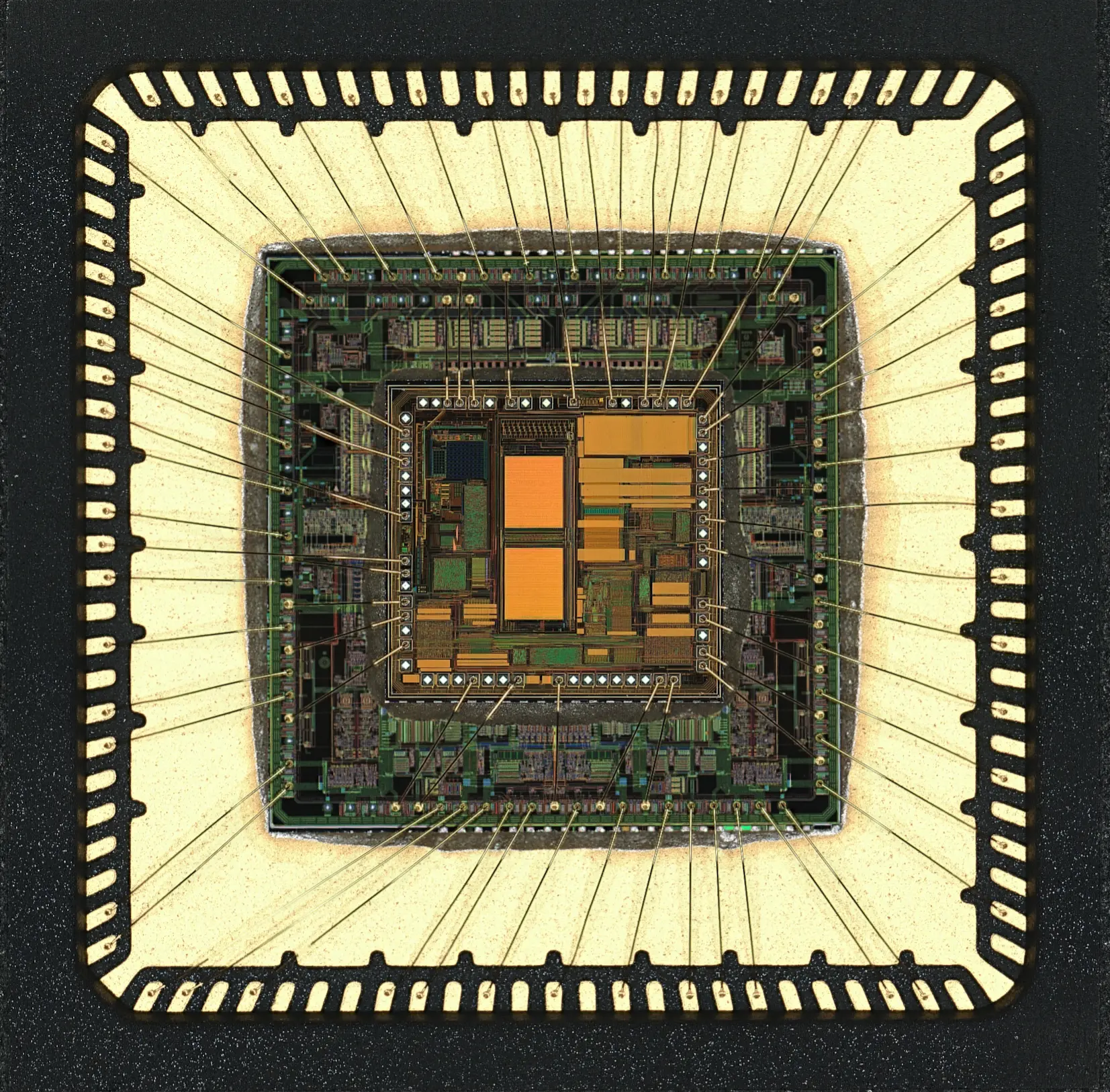
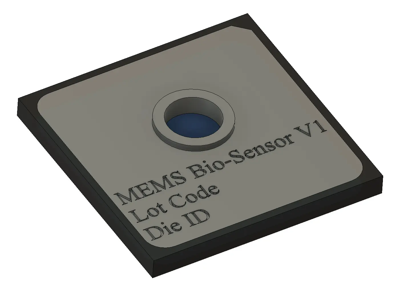
At Heisler Semiconductor LLC, we specialize in advanced semiconductor packaging prototyping services. Our expertise ensures that integrated circuits (ICs) are encased in protective packages that enhance functionality, reliability, and longevity. Our prototyping process is meticulously designed to optimize performance, manage costs, and accelerate time-to-market for your products.
Why Choose Our Semiconductor Package Prototyping service?
- Performance Optimization
- Electrical Efficiency: We ensure that your ICs operate at optimal speed and power levels.
- Thermal Management: Our designs effectively dissipate heat, preventing potential overheating issues.
- Mechanical Durability: We verify that our packages withstand physical stresses during operation and handling.
- Design Validation
- Precision Fit: We confirm that physical dimensions align perfectly with your application requirements.
- System Compatibility: Our packages are designed to integrate seamlessly with other system components.
- Cost Efficiency
- Material Selection: We help you choose cost-effective materials without compromising on quality.
- Manufacturing Budgeting: Our process includes accurate production cost estimations to refine your budgeting and pricing strategies.
- Accelerated Time-to-Market
- Early Issue Detection: We identify and resolve design and manufacturing challenges promptly.
- Process Optimization: Our refined manufacturing processes reduce production time, ensuring faster delivery.
Our Prototyping Process
To ensure the highest quality outcomes, we adhere to the following best practices:
- Comprehensive Planning
- Detailed Roadmap: We develop a clear roadmap outlining each step of the prototyping phase.
- Resource Allocation: Adequate resources are allocated to ensure timely and efficient project completion.
- Rigorous Testing
- Iterative Testing: Multiple testing iterations are conducted to identify and rectify issues early.
- Cross-functional Collaboration: We involve various departments, including design, engineering, and quality assurance, in the testing process.
- Effective Communication
- Regular Updates: We maintain consistent communication with all stakeholders to keep them informed of progress and any issues.
- Feedback Integration: A robust feedback loop is established to incorporate improvements swiftly.
- Advanced Prototyping Tools
- Simulation Software: We utilize advanced simulation tools to predict and optimize performance before creating physical prototypes.
- Rapid Prototyping Techniques: Our rapid prototyping methods allow for quick production and testing of early package versions.
- Supplier Collaboration
- Strategic Partnerships: We work closely with suppliers to ensure the timely delivery of high-quality materials and components.
- Joint Development Initiatives: Engaging in collaborative development activities allows us to leverage supplier expertise and innovation.
