GaN-on-SiC / Packaging + eval board design
Send us the die.
Get back a characterized board.
One offer, one team, one building: GaN-on-SiC packaging with the evaluation board, package substrate and interposer designed around your die — then attached, wire bonded, inspected and handed back ready for the bench.
/ Design / Substrate / Die attach / Wire bond / Inspection / US-soil
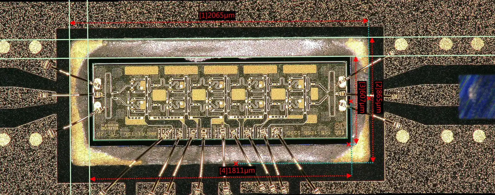
The whole thing,
under one roof.
Send us the die and the datasheet; get back a packaged part on a characterized eval board, designed, assembled, wire-bonded and inspected under one roof in the United States.
Most programs split this across three vendors: a design house draws the board, a fabricator builds it, an assembly shop attaches the die — and every constraint discovered at one of them becomes a purchase order and a schedule slip at the other two. Here the person who chooses the carrier is the person who runs the bonder, so a bond-finger problem is a layout revision the same week, not a returned lot.
Prototype and low-volume programs are welcome, and starting small does not cap where the program can go — assembly runs at 3,000 components per hour per system, on multiple systems.
The boundary
What we design. What we do not.
We design
RF evaluation boards, package substrates, interposers and chip-on-board test vehicles — the carrier, the stack-up, the launch, the bond fingers and the fixture the die lands on. See design & firmware for the full artifact list and the design rules we work to.
We do not design
The die. Heisler packages GaN-on-SiC die in the United States; we do not manufacture or design GaN die, and we do not design integrated circuits. You own the silicon. We own everything around it.
The route
Design, substrate, die attach, wire bond, inspection.
Six steps, one building. Every step below links to the page that carries its full detail, so nothing here is a summary of a claim made somewhere else.
Design
The evaluation board, package substrate or interposer, laid out around your pad map. Every release gets automated design-rule checking against the fabricator's own rule deck, run alongside the assembly rules, so fabrication and the bonder agree before anything is ordered. Design capability
Substrate and carrier
Aluminum nitride when heat is the argument, 96% alumina for thick-film ceramic, RO4003C or RT/duroid for low-loss laminate, polyimide build-up HDI for fine-line organic routing. Published Dk, Df, thermal conductivity and CTE for each: materials table
Die attach
AuSn eutectic and sintered silver are the usual GaN choices, picked by thermal budget; AuSi, AuGe, SnAg and silver-filled epoxy sit above and below them on the same temperature ladder. What is available depends on the die backside metallization. Process temperatures and when each wins: GaN alloy table
Wire bond
Thermosonic gold ball, ultrasonic aluminum wedge and ribbon, 15 to 50 µm fine wire, matched to the pad, the pitch and the current. Bond fingers are drawn to the same rules we bond to: substrate-side rule table
Inspection
X-ray for die-attach void content when void measurement is required, 3D automated optical inspection, and SEM. Wire bonds pull tested to MIL-STD-883 Method 2011. Inspection & metrology
Characterization hand-off
The board comes back with the part on it, the inspection records with it, and the bias and RF launch already exercised — so your first bench session measures the device, not the fixture.
Handling
ESD Class 0.
GaN and MMIC die are among the most static-sensitive parts anyone will ask you to handle, and the handling class is a screening question long before the packaging one.
Heisler has successfully run ESD Class 0 devices — the most sensitive human-body-model class in JEDEC JS-001, below 250 V HBM. Class 0 is a device sensitivity class, not a facility credential; Heisler claims no ESD certification.
Class definition: JEDEC JS-001 human-body model. Demonstrated experience, stated as experience.
To quote it
What we need from you.
- 01The die and its datasheet — or the datasheet first, if the die is still coming.
- 02Pad map and bond pad metallization — pad positions, sizes and pitch set the bond fingers and the escape routing.
- 03Die backside metallization — this is what decides which die-attach alloys are actually available to you.
- 04Bias and RF requirements — supply rails, frequency band, and what has to come out on a connector.
- 05Thermal budget — dissipation and the maximum junction temperature you can live with; this picks the carrier.
- 06What happens after the eval board — a characterization vehicle and a production package are not the same layout, and it is cheaper to know now.
Six inputs. Nothing else is needed for a first pass.
If some of that is still open, send what you have. Half the value of a first design review is finding out which of those six is actually the constraint.
Program-specific design rules, process windows and build data are available under NDA.
Start a design reviewQuestions engineers ask
GaN packaging and eval board design, answered.
What do I send you to start?
The die and its datasheet, plus the pad map and the bias and RF requirements. That is enough to lay out an evaluation board and pick a carrier. If the die is still in design, send the pad map when you have it and we will start on the carrier and the stack-up.
Does Heisler design the GaN die?
No. Heisler packages GaN-on-SiC die in the United States and designs the evaluation board, the package substrate and the interposer around it. We do not design or manufacture GaN die, or any other integrated circuit.
Can you handle ESD Class 0 parts?
Yes. Heisler has successfully run ESD Class 0 devices, the most sensitive human-body-model class in JEDEC JS-001, below 250 V HBM. Class 0 is a device sensitivity class, not a facility credential; Heisler claims no ESD certification.
Which carrier should a GaN-on-SiC die sit on?
Aluminum nitride is the usual answer, because its thermal conductivity is high and its expansion coefficient is close to the die. Published thermal conductivity and CTE for aluminum nitride, 96 percent alumina and the RF laminates are in the materials table, with the shear-strain comparison on the GaN packaging page.
What die attach do you use for GaN?
AuSn eutectic and sintered silver are the common choices, picked by thermal budget. The full cleared alloy set with process temperatures is on the GaN packaging page. What is attachable also depends on the die backside metallization, so send that with the datasheet.
How is the assembly verified before it ships?
X-ray for die-attach void content when void measurement is required, 3D automated optical inspection, and SEM. Wire bonds are pull tested to MIL-STD-883 Method 2011, where production typically runs three to four times the method minimum.
Is this only for production volume?
No. Prototype and low-volume programs are welcome, and starting small does not cap where the program can go. Assembly runs at 3,000 components per hour per system, on multiple systems, so the same process scales without being redeveloped.
Process More.
Send us the die
and the datasheet.
We will come back with a carrier, a stack-up and an evaluation board — then attach, bond, inspect and hand it back characterized. One team, one building, on US soil.
/ US-soil / traceable / NDA on request