
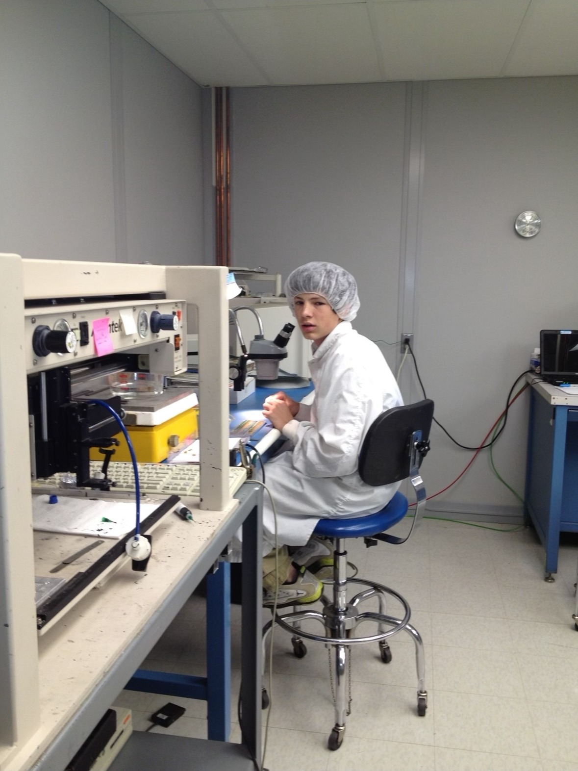
That's me at 12, back in 2007. Learning saw dicing, die bonding and wire bonding in a cleanroom.
I've been packaging semiconductors ever since.
It started in a basement
It started before that, in a basement. My grandfather Ed was a technician at Met-Ed, our local power utility, and he kept a workbench downstairs called the HAM Shack. From about six years old, that is where I was. He had me building circuit kits, tinning wire, wicking away a bad joint, checking my own work. I even rebuilt my broken PS3 motherboard in his basement. He took me to hamfest radio shows before I understood what they were. None of it felt like a career. It was just the thing my grandfather and I did.
My other grandfather, Nabil, came at it from the other end. He was a chemist in IBM's microelectronics division back in the 80s, and eventually joined my grandmother, Carol, an engineering manager at a lead frame and semiconductor packaging company, in the early 90s. In 2000 the two of them started their own microelectronics company, First Level. So I grew up with both halves of this industry in the family. The hands-on half in a basement, and the science half, packaging real semiconductors.
My first job was on the line
My first job was at First Level, and the photo above is one of the earliest I could find. I was an "engineering assistant" learning to dice, die bond, wire bond and inspect multichip modules. I must have reflowed hundreds of thousands of Cree semiconductor LEDs onto MCMs with up to 200 placements in a summer. Material quality, process repeatability and precision were critical. I was running calibration on Datacon BESI EVOs and other pick and place systems years before I could drive.
Real parts, real processes, at an age when most kids have not heard the words. I worked when I wasn't in school or sports, and I even learned the protocols for cleaning the cleanrooms. Quality products don't start with the product at all.
I grew up on the side where an idea turns into hardware. Where it gets bonded, sealed, tested and shipped, and where it fails if the process is wrong.
When I turned 18 I followed it the rest of the way. Electrical engineering at Catholic University of America, where I was the student chapter president of IEEE, then a master's at Johns Hopkins focused on solid state devices, geared toward learning circuit design from a packaging perspective. I worked at First Level as the engineering manager until 2024.
The gap I kept walking into
I can't tell you how many customer facilities I've walked into and seen bench-built production. Old school bonders, manual assembly, and process knowledge that lived in operators' heads. I saw a clear problem. The gap between volume manufacturing, with process cycle times in the low seconds per chip, and mid to low volume manufacturing, bench built, highly custom, often using technology developed in the 70s, 80s and 90s. A great example: DIPs on a "latest and greatest" device, leaving so much performance on the table. Copper loss, anyone?
I struggled to understand why such a gap existed, and then at 28 it finally clicked. I've spent so much of my career trying to train and develop a workforce on extremely complex equipment. One mistake could cost more than $100K on a production line. Packaging was not at the forefront of most companies' plans, it was an afterthought. The "make it work" mentality. I wanted to push the limits of technology. First Level wanted to run the tried and true processes the industry was built on. I wanted to make advanced electronics successfully on the first try, but the processes and equipment couldn't keep up.
It was an honest fork. First Level chose to stay on the proven side of manufacturing, with low financial risk. I wanted the work, and the risks, that they could not take. 3D heterogeneous integration, developing processes and equipment for next gen, AI in the process, real development where the outcome is not guaranteed. We wanted different things, and that was fine. I transitioned to an advisor and I am still deeply involved in their business.
Heisler Semiconductor, June 2024
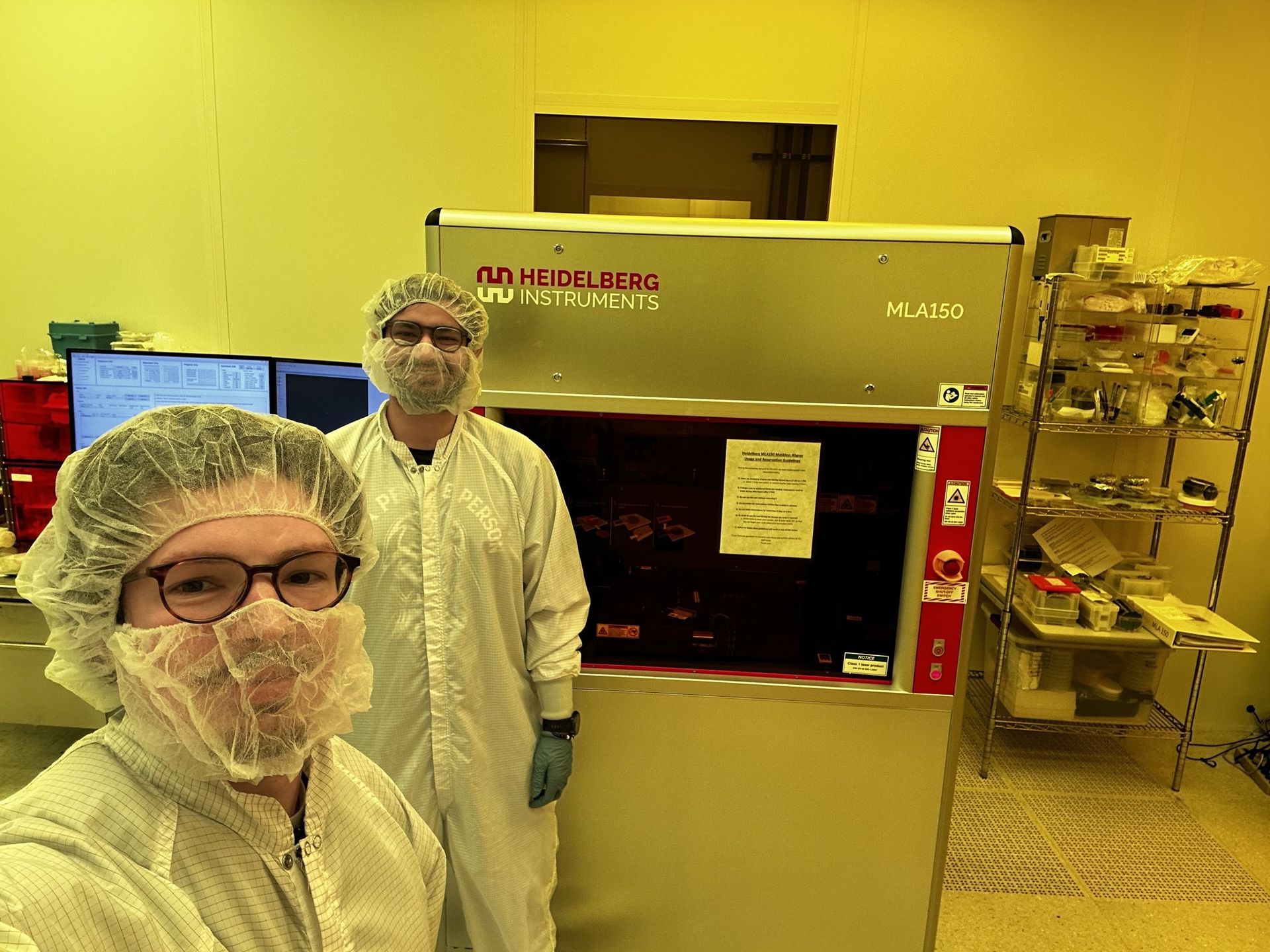
In June 2024 I started Heisler Semiconductor. This is now, at the maskless aligner in the nanofab center at the University of Maryland, with TJ. We use it to develop our wafer level packaging programs and substrates.
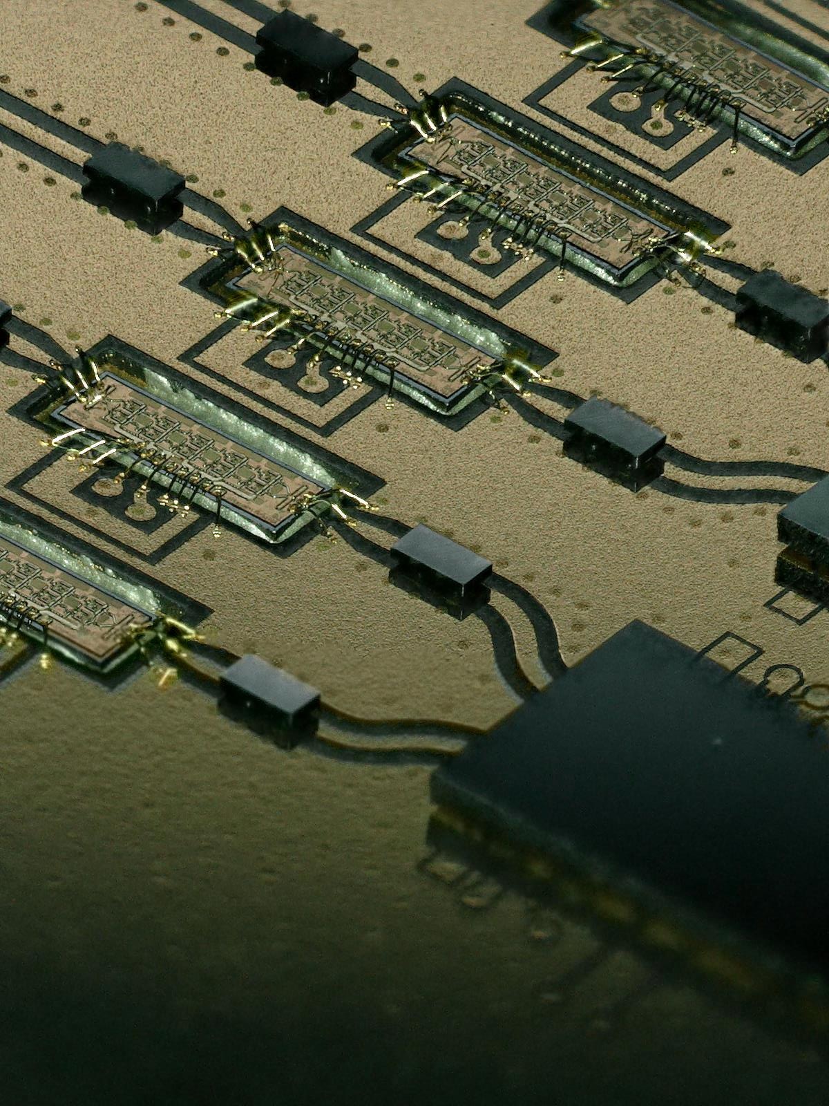
And this is the work. CMOS and InP die on one board, wire bonded, caps beside them. My team builds like this for customers every day, and we take on the hard, new work a risk-averse shop will not.
Same two threads my grandparents handed me. The hands and the science.
Same work, but on the bleeding edge, pushing the limit to bring the US market affordable and scalable solutions.